- 您现在的位置:买卖IC网 > PDF目录80516 > MK2048-01SLFTR 77.76 MHz, OTHER CLOCK GENERATOR, PDSO16 PDF资料下载
参数资料
| 型号: | MK2048-01SLFTR |
| 元件分类: | 时钟产生/分配 |
| 英文描述: | 77.76 MHz, OTHER CLOCK GENERATOR, PDSO16 |
| 封装: | 0.150 INCH, SOIC-16 |
| 文件页数: | 3/5页 |
| 文件大小: | 74K |
| 代理商: | MK2048-01SLFTR |
MK2048
Communications Frequency Generator
MDS 2048-01 B
3
Revision 022598
Printed 11/15/00
MicroClock Division of ICS1271 Parkmoor Ave.San JoseCA95126(408)295-9800tel(408)295-9818fax
PRELIMINARY INFORMATION
I C R O
C LOC K
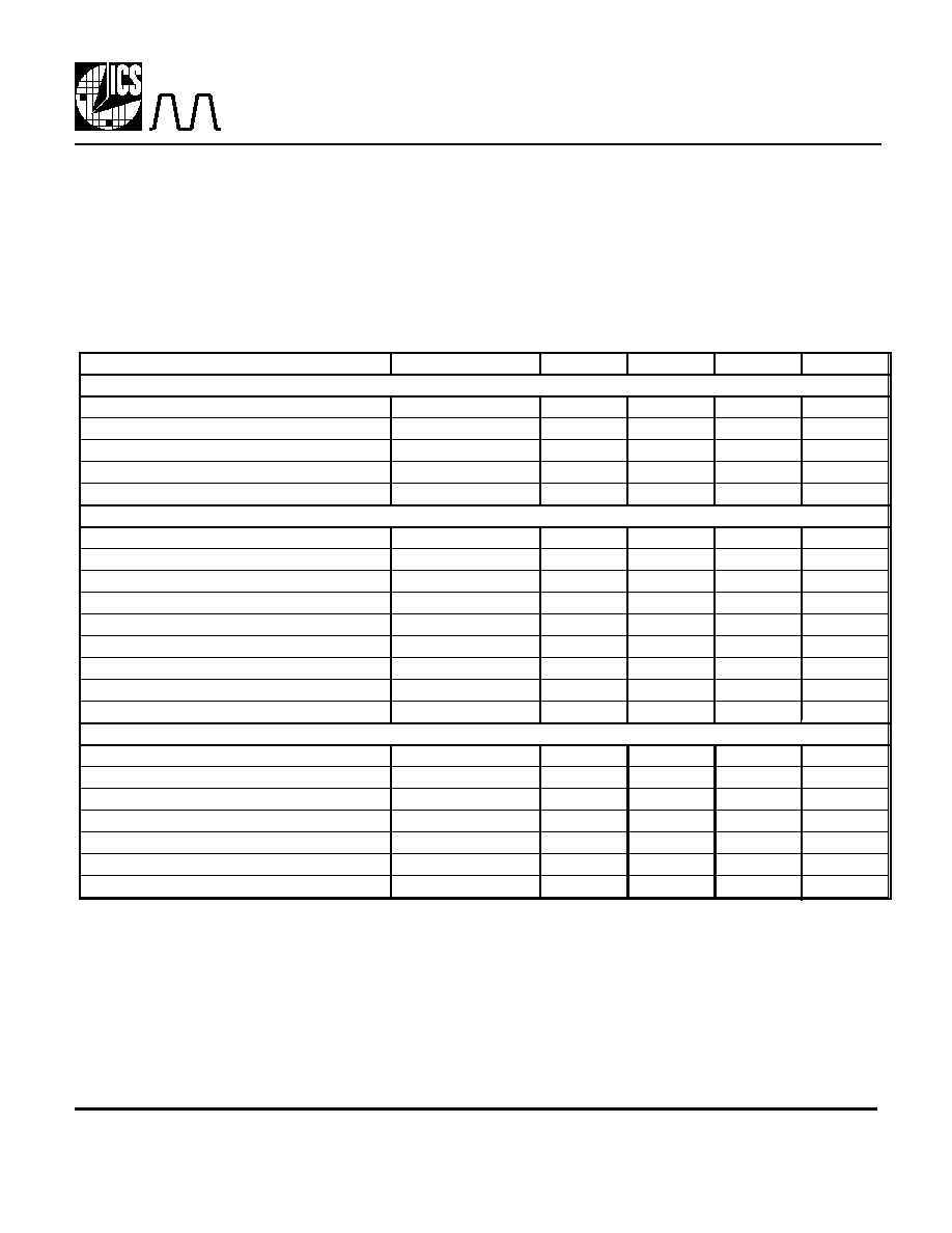
Parameter
Conditions
Minimum
Typical
Maximum
Units
ABSOLUTE MAXIMUM RATINGS (Note 1)
Supply Voltage, VDD
Referenced to GND
7
V
Inputs and Clock Outputs
-0.5
VDD+0.5
V
Ambient Operating Temperature
0
70
°C
Soldering Temperature
Max of 10 seconds
250
°C
Storage Temperature
-65
150
°C
DC CHARACTERISTICS (VDD = 5V unless noted)
Operating Voltage, VDD
4.5
5.5
V
Input High Voltage, VIH
2
V
Input Low Voltage, VIL
0.8
V
Output High Voltage
IOH=-4mA
VDD-0.4
V
Output High Voltage
IOH=-25mA
2.4
V
Output Low Voltage
IOL=25mA
0.4
V
Operating Supply Current, IDD
No Load, VDD=5.0V
15
mA
Short Circuit Current
Each output
±100
mA
Input Capacitance, FS3:0
7
pF
AC CHARACTERISTICS (VDD = 5V unless noted)
Input Frequency
ICLK
8.0000
kHz
Input Frequency
X1, X2
12.2880
MHz
Output Clock Rise Time
0.8 to 2.0V
1.5
ns
Output Clock Fall Time
2.0 to 0.8V
1.5
ns
Output Clock Duty Cycle, High Time
At VDD/2
40
49 to 51
60
%
Absolute Clock Period Jitter
TBD
ps
Actual mean frequency error versus target
Any clock selection
0
ppm
Notes:
1. Stresses beyond those listed under Absolute Maximum Ratings could cause permanent damage to the device. Prolonged exposure
to levels above the operating limits but below the Absolute Maximums may affect device reliability.
External Components/Crystal Selection
Electrical Specifications
The MK2048 requires a minimum number of external components for proper operation. An RC network
should be connected between CAP1 and CAP2 as close to the chip as possible. A high quality ceramic
capacitor is recommended, but leave provisions for sizes up to 10F. A decoupling capacitor of 0.1F must
be connected between VDD and GND pins (pins 2 and 3, 5 and 7) close to the chip, and 33
terminating
resistors can be used on clock outputs with traces longer than 1 inch.
相关PDF资料 |
PDF描述 |
|---|---|
| MC68HC11K4MFN2 | 8-BIT, MROM, 2 MHz, MICROCONTROLLER, PQCC84 |
| MC68HC711K4MFN4 | 8-BIT, OTPROM, 4 MHz, MICROCONTROLLER, PQCC84 |
| MC68L11K4FU3 | 8-BIT, MROM, 3 MHz, MICROCONTROLLER, PQFP80 |
| MPC8347EVRAGDA | 32-BIT, 400 MHz, MICROPROCESSOR, PBGA620 |
| MPC8349EVVALFA | 32-BIT, 667 MHz, MICROPROCESSOR, PBGA672 |
相关代理商/技术参数 |
参数描述 |
|---|---|
| MK2049-01 | 制造商:ICS 制造商全称:ICS 功能描述:Communications Clock PLL |
| MK2049-01S | 制造商:Integrated Device Technology Inc 功能描述:IC SM CLK GEN T1/E1/T3/E3 PLL 8KHZ P-SO- - Bulk |
| MK2049-01SI | 制造商:ICS 制造商全称:ICS 功能描述:Communications Clock PLL |
| MK2049-01SITR | 制造商:ICS 制造商全称:ICS 功能描述:Communications Clock PLL |
| MK2049-01STR | 制造商:Integrated Device Technology Inc 功能描述:PLL CLOCK SYNTHESIZER SGL 20SOIC - Tape and Reel |
发布紧急采购,3分钟左右您将得到回复。