- 您现在的位置:买卖IC网 > PDF目录132980 > MK2069-02GI 160 MHz, OTHER CLOCK GENERATOR, PDSO56 PDF资料下载
参数资料
| 型号: | MK2069-02GI |
| 元件分类: | 时钟产生/分配 |
| 英文描述: | 160 MHz, OTHER CLOCK GENERATOR, PDSO56 |
| 封装: | 6.10 MM, 0.50 MM PITCH, TSSOP-56 |
| 文件页数: | 15/20页 |
| 文件大小: | 347K |
| 代理商: | MK2069-02GI |
VCXO-Based Clock Jitter Attenuator and Translator
MDS 2069-02 G
4
Revision 050203
Integrated Circuit Systems, Inc. l 525 Race Street, San Jose, CA 95126 l tel (408) 295-9800 l
MK2069-02
Functional Description
The MK2069-02 is a PLL (Phase Locked Loop) based
clock generator that generates output clocks
synchronized to an input reference clock. It contains
two cascaded PLL’s with user selectable divider ratios.
The first PLL is VCXO-based and uses an external
pullable crystal as part of the normal “VCO” (voltage
controlled oscillator) function of the PLL. The use of a
VCXO assures a low phase noise clock source even
when a low PLL loop bandwidth is implemented. A low
loop bandwidth is needed when the input reference
frequency at the phase detector is low, or when jitter
attenuation of the input reference is desired.
The second PLL is used to translate or multiply the
frequency of the VCXO PLL which has a maximum
output frequency of 27 MHz. This second PLL, or
Translator PLL, uses an on-chip VCO circuit that can
provide an output clock up to 160 MHz. The Translator
PLL uses a high loop bandwidth (typically greater than
1 MHz) to assure stability of the clock output generated
by the VCO clock output. It requires a stable, high
frequency input reference which is provided by the
VCXO PLL.
The divide values of the divider blocks within both PLLs
are set by device pin configuration. This enables the
system designer to define the following:
Input clock frequency
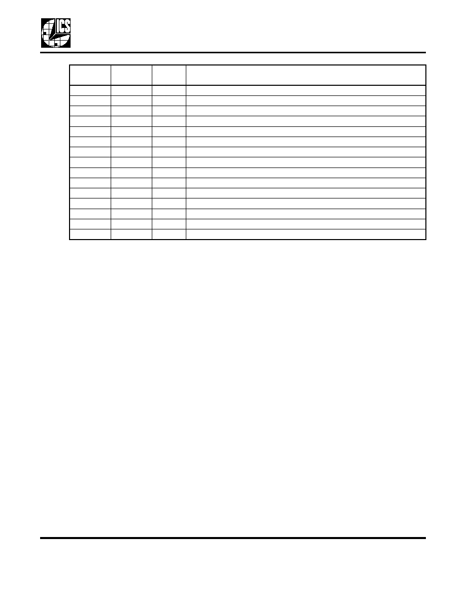
VCXO crystal frequency
VCLK output frequency
RCLK output frequency, which is also the phase
detector frequency of the VCXO PLL.
TCLK output frequency
Any unused clock or logic outputs can be tri-stated to
reduce interference (jitter, phase noise) on other clock
outputs. Outputs can also be tri-stated for system
testing purposes.
External components are used to configure the VCXO
PLL loop response. This serves to maximize loop
stability and to achieve the desired input clock jitter
attenuation characteristics.
42
VCLK
Output
Clock output from VCXO PLL
43
VDDP
Power
Power Supply for output drivers (VCLK, TCLK, RCLK, LD, LDR).
44
TCLK
Output
Clock output from Translator PLL
45
LD
Output
Lock detector output.
46
VDD
Power
Power Supply connection digital circuitry.
47
OER
Input
Output enable for RCLK. RCLK is tri-stated when low, internal pull-up.
48
OEV
Input
Output enable for VCLK. VCLK is tri-stated when low, internal pull-up.
49
OET
Input
Output enable for TCLK. TCLK is tri-stated when low, internal pull-up.
50
OEL
Input
Output enable for LD. LD is tri-stated when low, internal pull-up.
51
PV2
Input
Phase Detector Divider bit 2, VCXO PLL, internal pull-up.
52
PV3
Input
Phase Detector Divider bit 3, VCXO PLL, internal pull-up.
53
PV4
Input
Phase Detector Divider bit 4, VCXO PLL, internal pull-up.
54
SV0
Input
Scaler Divider bit 0 input, VCXO PLL, internal pull-up.
55
SV1
Input
Scaler Divider bit 1 input, VCXO PLL, internal pull-up.
56
SV2
Input
Scaler Divider bit 2 input, VCXO PLL, internal pull-up.
Pin
Number
Pin
Name
Pin
Type
Pin Description
相关PDF资料 |
PDF描述 |
|---|---|
| MC68882CFN16A | 32-BIT, MATH COPROCESSOR, PQCC68 |
| MC68882CFN20A | 32-BIT, MATH COPROCESSOR, PQCC68 |
| MC68882CFN33A | 32-BIT, MATH COPROCESSOR, PQCC68 |
| MC68882CRC20A | 32-BIT, MATH COPROCESSOR, CPGA68 |
| MC68882CRC33A | 32-BIT, MATH COPROCESSOR, CPGA68 |
相关代理商/技术参数 |
参数描述 |
|---|---|
| MK2069-03 | 制造商:ICS 制造商全称:ICS 功能描述:VCXO-Based Clock Translator with High Multiplication |
| MK2069-03GI | 功能描述:IC VCXO CLK TRANSLATOR 56-TSSOP RoHS:否 类别:集成电路 (IC) >> 时钟/计时 - 时钟发生器,PLL,频率合成器 系列:- 标准包装:27 系列:Precision Edge® 类型:频率合成器 PLL:是 输入:PECL,晶体 输出:PECL 电路数:1 比率 - 输入:输出:1:1 差分 - 输入:输出:无/是 频率 - 最大:800MHz 除法器/乘法器:是/无 电源电压:3.135 V ~ 5.25 V 工作温度:0°C ~ 85°C 安装类型:表面贴装 封装/外壳:28-SOIC(0.295",7.50mm 宽) 供应商设备封装:28-SOIC 包装:管件 |
| MK2069-03GITR | 功能描述:时钟发生器及支持产品 VCXO-BASED CLOCK TRANSLATOR RoHS:否 制造商:Silicon Labs 类型:Clock Generators 最大输入频率:14.318 MHz 最大输出频率:166 MHz 输出端数量:16 占空比 - 最大:55 % 工作电源电压:3.3 V 工作电源电流:1 mA 最大工作温度:+ 85 C 安装风格:SMD/SMT 封装 / 箱体:QFN-56 |
| MK2069-04 | 制造商:ICS 制造商全称:ICS 功能描述:VCXO-Based Universal Clock Translator |
| MK2069-04GI | 功能描述:IC VCXO CLK TRANSLATOR 56-TSSOP RoHS:否 类别:集成电路 (IC) >> 时钟/计时 - 时钟发生器,PLL,频率合成器 系列:- 标准包装:39 系列:- 类型:* PLL:带旁路 输入:时钟 输出:时钟 电路数:1 比率 - 输入:输出:1:10 差分 - 输入:输出:是/是 频率 - 最大:170MHz 除法器/乘法器:无/无 电源电压:2.375 V ~ 3.465 V 工作温度:0°C ~ 70°C 安装类型:* 封装/外壳:* 供应商设备封装:* 包装:* |
发布紧急采购,3分钟左右您将得到回复。