- 您现在的位置:买卖IC网 > PDF目录45328 > MK2069-03GITR (INTEGRATED DEVICE TECHNOLOGY INC) 160 MHz, OTHER CLOCK GENERATOR, PDSO56 PDF资料下载
参数资料
| 型号: | MK2069-03GITR |
| 厂商: | INTEGRATED DEVICE TECHNOLOGY INC |
| 元件分类: | 时钟产生/分配 |
| 英文描述: | 160 MHz, OTHER CLOCK GENERATOR, PDSO56 |
| 封装: | 6.10 MM, 0.50 MM PITCH, TSSOP-56 |
| 文件页数: | 18/20页 |
| 文件大小: | 204K |
| 代理商: | MK2069-03GITR |
MK2069-03
VCXO-BASED CLOCK TRANSLATOR WITH HIGH MULTIPLICATION
VCXO AND SYNTHESIZER
IDT / ICS VCXO-BASED CLOCK TRANSLATOR WITH HIGH MULTIPLICATION 7
MK2069-03
REV J 030906
CP establishes a second pole in the VCXO PLL loop filter.
For higher damping factors (> 1), calculate the value of CP
based on a CS value that would be used for a damping factor
of 1. This will minimize baseband peaking and loop
instability that can lead to output jitter.
CP also dampens VCXO input voltage modulation by the
charge pump correction pulses. A CP value that is too low
will result in increased output phase noise at the phase
detector frequency due to this. In extreme cases where
input jitter is high, charge pump current is high, and CP is too
small, the VCXO input voltage can hit the supply or ground
rail resulting in non-linear loop response.
The best way to set the value of CP is to use the filter
response software available from ICS (please refer to the
following section). CP should be increased in value until it
just starts affecting the passband peak.
Loop Filter Response Software
Online tools to calculate loop filter response can be found at
www.idt.com/?app=calculators&source=support_menu.
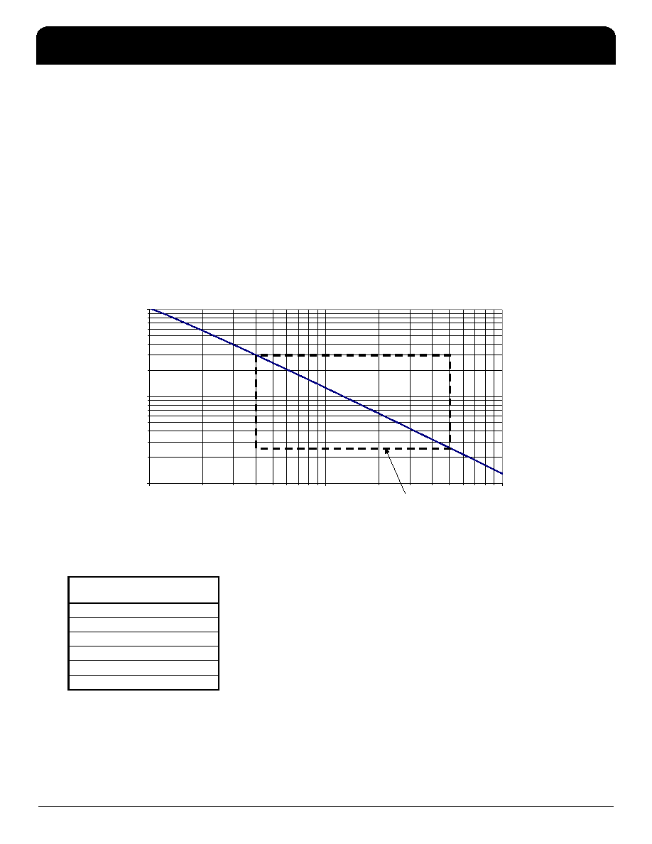
Graph of Charge Pump Current vs. Value of RSET (external resistor)
Charge Pump Current, Example Settings from
Above Graph
Notes on Setting Charge Pump Current
The recommended range for the charge pump current is 25
μA to 300 μA. Below 25 μA, loop filter charge leakage, due
to PCB or capacitor leakage, can become a problem. This
loop filter leakage can cause locking problems, output clock
cycle slips, or low frequency phase noise.
As can be seen in the loop bandwidth and damping factor
equations or by using the filter response software available
from ICS, increasing charge pump current (ICP) increases
both bandwidth and damping factor.
C
P
C
S
20
------
=
10E-6
100E-6
1E-3
100E+3
1E+6
10E+6
RSET, ohms
I CP
,A
m
ps
Recommended Range
of Operation
RSET
Charge Pump Current
(ICP)
5 M
Ω
25
μA
3 M
Ω
42
μA
2 M
Ω
65
μA
1 M
Ω
125
μA
480 k
Ω
255
μA
400 k
Ω
300
μA
相关PDF资料 |
PDF描述 |
|---|---|
| MK2069-03GITR | 160 MHz, OTHER CLOCK GENERATOR, PDSO56 |
| MK2069-04GITR | 160 MHz, OTHER CLOCK GENERATOR, PDSO56 |
| MK2069-04GI | 160 MHz, OTHER CLOCK GENERATOR, PDSO56 |
| MK20DN512ZVLL10 | RISC MICROCONTROLLER, PQFP100 |
| MK20DN512ZVLQ10 | 32-BIT, FLASH, 100 MHz, RISC MICROCONTROLLER, PQFP144 |
相关代理商/技术参数 |
参数描述 |
|---|---|
| MK2069-04 | 制造商:ICS 制造商全称:ICS 功能描述:VCXO-Based Universal Clock Translator |
| MK2069-04GI | 功能描述:IC VCXO CLK TRANSLATOR 56-TSSOP RoHS:否 类别:集成电路 (IC) >> 时钟/计时 - 时钟发生器,PLL,频率合成器 系列:- 标准包装:39 系列:- 类型:* PLL:带旁路 输入:时钟 输出:时钟 电路数:1 比率 - 输入:输出:1:10 差分 - 输入:输出:是/是 频率 - 最大:170MHz 除法器/乘法器:无/无 电源电压:2.375 V ~ 3.465 V 工作温度:0°C ~ 70°C 安装类型:* 封装/外壳:* 供应商设备封装:* 包装:* |
| MK2069-04GILF | 功能描述:时钟发生器及支持产品 VCXO-BASED UNIVERSAL CLOCK TRANSLATOR RoHS:否 制造商:Silicon Labs 类型:Clock Generators 最大输入频率:14.318 MHz 最大输出频率:166 MHz 输出端数量:16 占空比 - 最大:55 % 工作电源电压:3.3 V 工作电源电流:1 mA 最大工作温度:+ 85 C 安装风格:SMD/SMT 封装 / 箱体:QFN-56 |
| MK2069-04GILFTR | 功能描述:时钟发生器及支持产品 VCXO-BASED UNIVERSAL CLOCK TRANSLATOR RoHS:否 制造商:Silicon Labs 类型:Clock Generators 最大输入频率:14.318 MHz 最大输出频率:166 MHz 输出端数量:16 占空比 - 最大:55 % 工作电源电压:3.3 V 工作电源电流:1 mA 最大工作温度:+ 85 C 安装风格:SMD/SMT 封装 / 箱体:QFN-56 |
| MK2069-04GITR | 功能描述:IC VCXO CLK TRANSLATOR 56-TSSOP RoHS:否 类别:集成电路 (IC) >> 时钟/计时 - 时钟发生器,PLL,频率合成器 系列:- 标准包装:39 系列:- 类型:* PLL:带旁路 输入:时钟 输出:时钟 电路数:1 比率 - 输入:输出:1:10 差分 - 输入:输出:是/是 频率 - 最大:170MHz 除法器/乘法器:无/无 电源电压:2.375 V ~ 3.465 V 工作温度:0°C ~ 70°C 安装类型:* 封装/外壳:* 供应商设备封装:* 包装:* |
发布紧急采购,3分钟左右您将得到回复。