- 您现在的位置:买卖IC网 > PDF目录45333 > ML67Q5002LA (OKI ELECTRIC INDUSTRY CO LTD) 32-BIT, FLASH, 60 MHz, RISC MICROCONTROLLER, PBGA144 PDF资料下载
参数资料
| 型号: | ML67Q5002LA |
| 厂商: | OKI ELECTRIC INDUSTRY CO LTD |
| 元件分类: | 微控制器/微处理器 |
| 英文描述: | 32-BIT, FLASH, 60 MHz, RISC MICROCONTROLLER, PBGA144 |
| 封装: | 11 X 11 MM, 0.80 MM PITCH, PLASTIC, LFBGA-144 |
| 文件页数: | 5/20页 |
| 文件大小: | 650K |
| 代理商: | ML67Q5002LA |
Oki Semiconductor 13
ML675001/ML67Q5002/ML67Q5003
April 2004, Rev 2.0
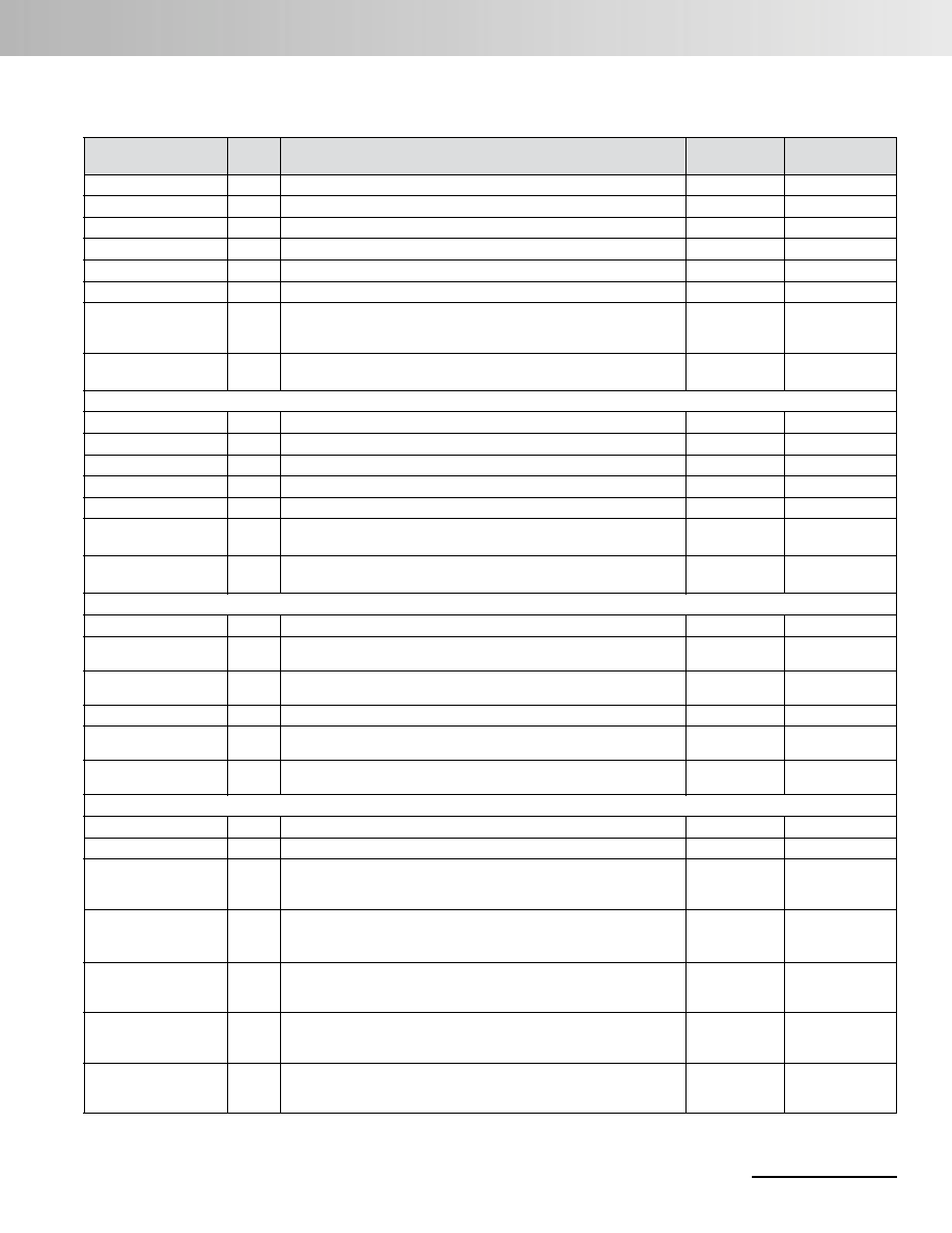
XIOCS_N[3]
O
I/O chip select 3.
–
Negative
XOE_N
O
Output enable/ Read enable.
–
Negative
XWE_N
O
Write enable.
–
Negative
XBS_N[1:0]
O
Byte select: XBS_N[1] is for MSB, XBS_N[0] is for LSB.
–
Negative
XBWE_N[0]
O
LSB Write enable.
–
Negative
XBWE_N[1]
O
MSB Write enable.
–
Negative
XWR
O
Data transfer direction for external bus, used when connecting to Motorola I/O devices. This
represent the secondary function of pin PIOC[7].
L = read, H = write. Available for I/O bank 0/1
Secondary
–
XWAIT
I
External I/O bank 0/1/2/3 WAIT signal.
This pin permits access to devices slower than register settings.
Secondary
Positive
External Bus Interface (EDO-DRAM and SDRAM)
XRAS_N
O
Row address strobe. Used for both EDO DRAM and SDRAM.
Secondary
Negative
XCAS_N
O
Column address strobe signal (SDRAM).
Secondary
Negative
XSDCLK
O
SDRAM clock (same frequency as internal system clock).
Secondary
–
XSDCKE
O
Clock enable (SDRAM).
Secondary
–
XSDCS_N
O
Chip select (SDRAM).
Secondary
Negative
XDQM[1]/
XCAS_N[1]
O
Connected to SDRAM: DQM (MSB).
Connected to EDO-DRAM: column address strobe signal (MSB).
Secondary
Positive
Negative
XDQM[0]/
XCAS_N[0]
O
Connected to SDRAM: DQM (LSB).
Connected to EDO-DRAM: column address strobe signal (LSB).
Secondary
Positive
Negative
DMA Interface
DREQ[0]
I
Channel 0 DMA request signal. Used then DMA controller is congured for DREQ type.
Secondary
Positive
DREQCLR[0]
O
Channel 0 DREQ signal clear request. The DMA device responds to the assertion of this sig-
nal by negating DREQ.
Secondary
Positive
TCOUT[0]
O
This signal is driven by the MCU and indicates to the Channel 0 DMA device that the last
transfer of the DMA operation has started.
Secondary
Positive
DREQ[1]
I
Channel 1 DMA request signal. Used then DMA controller is congured for DREQ type.
Secondary
Positive
DREQCLR[1]
O
Channel 1 DREQ signal clear request. The DMA device responds to the assertion of this sig-
nal by negating DREQ.
Secondary
Positive
TCOUT[1]
O
This signal is driven by the MCU and indicates to the Channel 1 DMA device that the last
transfer of the DMA operation has started.
Secondary
Positive
UART Interface
SIN
I
UART receive signal.
Secondary
Positive
SOUT
O
UART transmit signal.
Secondary
Positive
CTS
I
Clear To Send.
Indicates that modem or data set is ready to transfer data. Bit 4 in the modem status reg-
ister reects this input.
Secondary
Negative
DSR
I
Data Set Ready.
Indicates that modem or data set is ready to establish a communications link with UART.
Bit 5 in the modem status register reects this input.
Secondary
Negative
DCD
I
Data Carrier Detect.
Indicates that modem or data set has detected data carrier signal.Bit 7 in the modem status
register reects this input.
Secondary
Negative
DTR
O
Data Terminal Ready.
Indicates that UART is ready to establish a communications link with the modem or data set.
Bit 0 in the modem control register controls this output.
Secondary
Negative
RTSO
Request To Send.
indicates that UART is ready to transfer data to modem or data set. Bit 1 in the modem con-
trol register controls this output.
Secondary
Negative
Pin Descriptions (Continued)
Pin Name
I/O
Description
Primary/
Secondary
Logic
相关PDF资料 |
PDF描述 |
|---|---|
| ML675001LA | 32-BIT, 60 MHz, RISC MICROCONTROLLER, PBGA144 |
| ML67Q5003TC | 32-BIT, FLASH, 60 MHz, RISC MICROCONTROLLER, PQFP144 |
| ML675001TC | 32-BIT, 60 MHz, RISC MICROCONTROLLER, PQFP144 |
| ML67Q5002TC | 32-BIT, FLASH, 60 MHz, RISC MICROCONTROLLER, PQFP144 |
| ML67Q5002LA | 32-BIT, FLASH, 60 MHz, RISC MICROCONTROLLER, PBGA144 |
相关代理商/技术参数 |
参数描述 |
|---|---|
| ML67Q5002-NNNLA | 制造商:ROHM Semiconductor 功能描述: |
| ML67Q5002-NNNTC | 制造商:ROHM Semiconductor 功能描述: |
| ML67Q5002TC | 制造商:ROHM Semiconductor 功能描述: |
| ML67Q5003 | 制造商:OKI 制造商全称:OKI electronic componets 功能描述:32-bit ARM-Based General-Purpose Microcontroller |
| ML67Q5003ALA | 制造商:ROHM Semiconductor 功能描述: |
发布紧急采购,3分钟左右您将得到回复。