- 您现在的位置:买卖IC网 > PDF目录80482 > MM908E624ACEW/R2 (FREESCALE SEMICONDUCTOR INC) 8-BIT, FLASH, 32 MHz, MICROCONTROLLER, PDSO54 PDF资料下载
参数资料
| 型号: | MM908E624ACEW/R2 |
| 厂商: | FREESCALE SEMICONDUCTOR INC |
| 元件分类: | 微控制器/微处理器 |
| 英文描述: | 8-BIT, FLASH, 32 MHz, MICROCONTROLLER, PDSO54 |
| 封装: | 0.65 MM PITCH, ROHS COMPLIANT, SOIC-54 |
| 文件页数: | 17/39页 |
| 文件大小: | 702K |
| 代理商: | MM908E624ACEW/R2 |
第1页第2页第3页第4页第5页第6页第7页第8页第9页第10页第11页第12页第13页第14页第15页第16页当前第17页第18页第19页第20页第21页第22页第23页第24页第25页第26页第27页第28页第29页第30页第31页第32页第33页第34页第35页第36页第37页第38页第39页
Analog Integrated Circuit Device Data
24
Freescale Semiconductor
908E624
FUNCTIONAL DEVICE OPERATION
OPERATIONAL MODES
disconnected from VSUP and a small current source keeps
the LIN pin in recessive state. The receiver is still active to be
able to detect wake-up events on the LIN bus line.
A dominant level longer than tPROPWL followed by an rising
edge will generate a system wake-up (reset) and set the
LINWF flag in the SPI Status Register. Also see Figure 8,
WINDOW WATCHDOG
The window watchdog is configurable using an external
resistor at the WDCONF pin. The watchdog is cleared
through by the MODE1:2 bits in the SPI Control register (refer
to Table 8, page 26).
A watchdog clear is only allowed in the open window. If the
watchdog is cleared in the closed window or has not been
cleared at the end of the open window, the watchdog will
generate a reset on the RST_A pin and reset the whole
device.
Note
The watchdog clear in Normal request mode
(150 ms) (first watchdog clear) has no window.
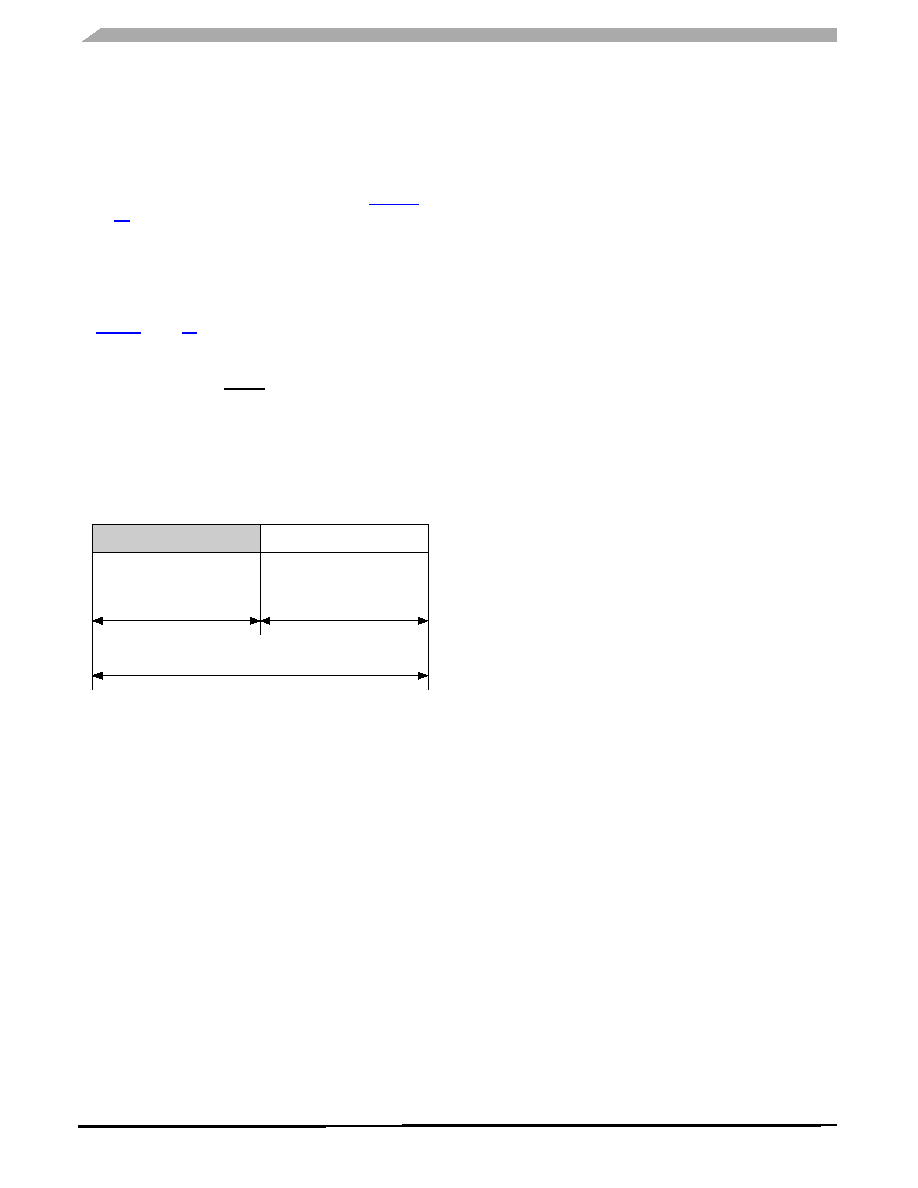
Figure 16. Window Watchdog Operation
Watchdog Configuration
If the WDCONF pin is left open, the default watchdog
period is selected (typ. 150 ms). If no watchdog function is
required, the WDCONF pin must be connected to GND.
The watchdog period is calculated using the following
formula:
tPWD [ms] = 0.991 * REXT [kΩ] + 0.648
VOLTAGE REGULATOR
The 908E624 chip contains a low-power, low dropout
voltage regulator to provide internal power and external
power for the MCU. The on-chip regulator consist of two
elements, the main voltage regulator and the low-voltage
reset circuit.
The VDD regulator accepts an unregulated input supply
and provides a regulated VDD supply to all digital sections of
the device. The output of the regulator is also connected to
the VDD pin to provide the 5.0 V to the microcontroller.
Current Limit (Over-current) Protection
The voltage regulator has current limit to protect the device
against over-current and short-circuit conditions.
Over-temperature Protection
The voltage regulator also features an over-temperature
protection having an over-temperature warning (Interrupt -
VDDT) and an over-temperature shutdown.
Stop Mode
During Stop mode, the Stop mode regulator supplies a
regulated output voltage. The Stop mode regulator has a
limited output current capability.
Sleep Mode
In Sleep mode the voltage regulator external VDD is turned
off.
FACTORY TRIMMING AND CALIBRATION
To enhance the ease of use of the 908E624, various
parameters (e.g., ICG trim value) are stored in the flash
memory of the device. The following flash memory locations
are reserved for this purpose and might have a value different
from the “empty” (0xFF) state:
0xFD80:0xFDDF Trim and Calibration Values
0xFFFE:0xFFFF Reset Vector
In the event the application uses these parameters, one
has to take care not to erase or override these values. If these
parameters are not used, these flash locations can be erased
and otherwise used.
Trim Values
The usage of the trim values, located in the flash memory,
is explained in the following.
Internal Clock Generator (ICG) Trim Value
The internal clock generator (ICG) module is used to
create a stable clock source for the microcontroller without
using any external components. The untrimmed frequency of
the low frequency base clock (IBASE), will vary as much as
±25%, due to process, temperature, and voltage
dependencies. To compensate for these dependencies, an
ICG trim value is located at the address $FDC2. After
trimming the ICG, a range of typ. ±2% (±3% max.) at nominal
conditions (filtered (100 nF) and stabilized (4.7
μF) VDD =
5.0 V, TAmbient~23 °C) and will vary over-temperature and
voltage (VDD) as indicated in the 68HC908EY16 data sheet.
To trim the ICG, these values must be copied to the ICG
Trim Register ICGTR at address $38 of the MCU.
Important
The value has to be copied after every reset.
OPERATING MODES OF THE MCU
For a detailed description of the operating modes of the
MCU, refer to the MC68HC908EY16 data sheet.
Window closed
no watchdog clear allowed
Window open
for watchdog clear
WD timing x 50%
WD period (PWD)
WD timing selected by resistor on WDCONF terminal.
(tPWD)
相关PDF资料 |
PDF描述 |
|---|---|
| MSP430CG4617IPZ | 16-BIT, FLASH, 8 MHz, RISC MICROCONTROLLER, PQFP100 |
| MC9328MX21SCVK | 32-BIT, 266 MHz, MICROPROCESSOR, PBGA289 |
| MC7457RX1200LC | 32-BIT, 1200 MHz, RISC PROCESSOR, CBGA483 |
| MC3S12HZ32J3CAA | 16-BIT, MROM, 25 MHz, MICROCONTROLLER, PQFP80 |
| MC9S12HZ64J3MAA | 16-BIT, FLASH, 25 MHz, MICROCONTROLLER, PQFP80 |
相关代理商/技术参数 |
参数描述 |
|---|---|
| MM908E624ACPEW | 功能描述:8位微控制器 -MCU 3 HIGH SIDE SWITCH RoHS:否 制造商:Silicon Labs 核心:8051 处理器系列:C8051F39x 数据总线宽度:8 bit 最大时钟频率:50 MHz 程序存储器大小:16 KB 数据 RAM 大小:1 KB 片上 ADC:Yes 工作电源电压:1.8 V to 3.6 V 工作温度范围:- 40 C to + 105 C 封装 / 箱体:QFN-20 安装风格:SMD/SMT |
| MM908E624ACPEWR2 | 功能描述:8位微控制器 -MCU 3 HIGH SIDE DRIVER RoHS:否 制造商:Silicon Labs 核心:8051 处理器系列:C8051F39x 数据总线宽度:8 bit 最大时钟频率:50 MHz 程序存储器大小:16 KB 数据 RAM 大小:1 KB 片上 ADC:Yes 工作电源电压:1.8 V to 3.6 V 工作温度范围:- 40 C to + 105 C 封装 / 箱体:QFN-20 安装风格:SMD/SMT |
| MM908E624AYEW | 功能描述:开关 IC - 各种 TRIPLE HIGH SIDE SWITCH RoHS:否 制造商:Fairchild Semiconductor 开启电阻(最大值): 电源电压-最大:4.4 V 电源电压-最小:2.5 V 最大工作温度:+ 85 C 最小工作温度:- 40 C 封装 / 箱体:WLCSP-9 封装:Reel |
| MM908E624AYEW/R2 | 制造商:FREESCALE 制造商全称:Freescale Semiconductor, Inc 功能描述:Integrated Triple High Side Switch with Embedded MCU and LIN Serial Communicationfor Relay Drivers |
| MM908E624AYEWR2 | 功能描述:开关 IC - 各种 TRIPLE HIGH SIDE SWITCH RoHS:否 制造商:Fairchild Semiconductor 开启电阻(最大值): 电源电压-最大:4.4 V 电源电压-最小:2.5 V 最大工作温度:+ 85 C 最小工作温度:- 40 C 封装 / 箱体:WLCSP-9 封装:Reel |
发布紧急采购,3分钟左右您将得到回复。