- 您现在的位置:买卖IC网 > PDF目录95978 > MMDF7N02ZR2 (MOTOROLA INC) 7000 mA, 20 V, 2 CHANNEL, N-CHANNEL, Si, SMALL SIGNAL, MOSFET PDF资料下载
参数资料
| 型号: | MMDF7N02ZR2 |
| 厂商: | MOTOROLA INC |
| 元件分类: | 小信号晶体管 |
| 英文描述: | 7000 mA, 20 V, 2 CHANNEL, N-CHANNEL, Si, SMALL SIGNAL, MOSFET |
| 文件页数: | 1/10页 |
| 文件大小: | 190K |
| 代理商: | MMDF7N02ZR2 |
1
Motorola TMOS Power MOSFET Transistor Device Data
Advance Information
Medium Power Surface Mount Products
TMOS Dual N-Channel with
Monolithic Zener ESD Protected Gate
EZFETs
are an advanced series of power MOSFETs which
utilize Motorola’s High Cell Density TMOS process and contain
monolithic back–to–back zener diodes. These zener diodes
provide protection against ESD and unexpected transients. These
miniature surface mount MOSFETs feature ultra low RDS(on) and
true logic level performance. They are capable of withstanding high
energy in the avalanche and commutation modes and the
drain–to–source diode has a very low reverse recovery time.
EZFET devices are designed for use in low voltage, high speed
switching applications where power efficiency is important. Typical
applications are dc–dc converters, and power management in
portable and battery powered products such as computers,
printers, cellular and cordless phones. They can also be used for
low voltage motor controls in mass storage products such as disk
drives and tape drives.
Zener Protected Gates Provide Electrostatic Discharge Protection
Designed to Withstand 200 V Machine Model and 2000 V Human Body Model
Ultra Low RDS(on) Provides Higher Efficiency and Extends Battery Life
Logic Level Gate Drive — Can Be Driven by Logic ICs
Miniature SO–8 Surface Mount Package — Saves Board Space
Diode Is Characterized for Use In Bridge Circuits
Diode Exhibits High Speed, With Soft Recovery
IDSS Specified at Elevated Temperature
Mounting Information for SO–8 Package Provided
MAXIMUM RATINGS (TJ = 25°C unless otherwise noted)
Parameter
Symbol
Max
Unit
Drain–to–Source Voltage
VDSS
20
Vdc
Drain–to–Gate Voltage (RGS = 1.0 M)
VDGR
20
Vdc
Gate–to–Source Voltage — Continuous
VGS
± 12
Vdc
Drain Current — Continuous @ TA = 25°C (1)
Drain Current — Continuous @ TA = 70°C (1)
Drain Current — Pulsed Drain Current (3)
ID
IDM
7.0
4.6
35
Adc
Total Power Dissipation @ TA = 25°C (1)
Linear Derating Factor @ TA = 25°C (1)
PD
2.0
16
Watts
mW/
°C
Total Power Dissipation @ TA = 25°C (2)
Linear Derating Factor @ TA = 25°C (2)
PD
1.39
11.11
Watts
mW/
°C
Operating and Storage Temperature Range
TJ, Tstg
– 55 to 150
°C
THERMAL RESISTANCE
Parameter
Symbol
Typ
Max
Unit
Junction–to–Ambient (1)
Junction–to–Ambient (2)
RqJA
—
62.5
90
°C/W
(1) When mounted on 1” square FR4 or G–10 board (VGS = 10 V, @ 10 seconds).
(2) When mounted on minimum recommended FR4 or G–10 board (VGS = 10 V, @ Steady State).
(3) Repetitive rating; pulse width limited by maximum junction temperature.
DEVICE MARKING
ORDERING INFORMATION
D7N02Z
Device
Reel Size
Tape Width
Quantity
D7N02Z
MMDF7N02ZR2
13
″
12 mm embossed tape
2500 units
This document contains information on a new product. Specifications and information herein are subject to change without notice.
HDTMOS is a trademark of Motorola, Inc. TMOS is a registered trademark of Motorola, Inc.
Thermal Clad is a trademark of the Bergquist Company.
Preferred devices are Motorola recommended choices for future use and best overall value.
Order this document
by MMDF7N02Z/D
MOTOROLA
SEMICONDUCTOR TECHNICAL DATA
Motorola, Inc. 1997
Source–1
1
2
3
4
8
7
6
5
Top View
Gate–1
Source–2
Gate–2
Drain–1
Drain–2
D
S
G
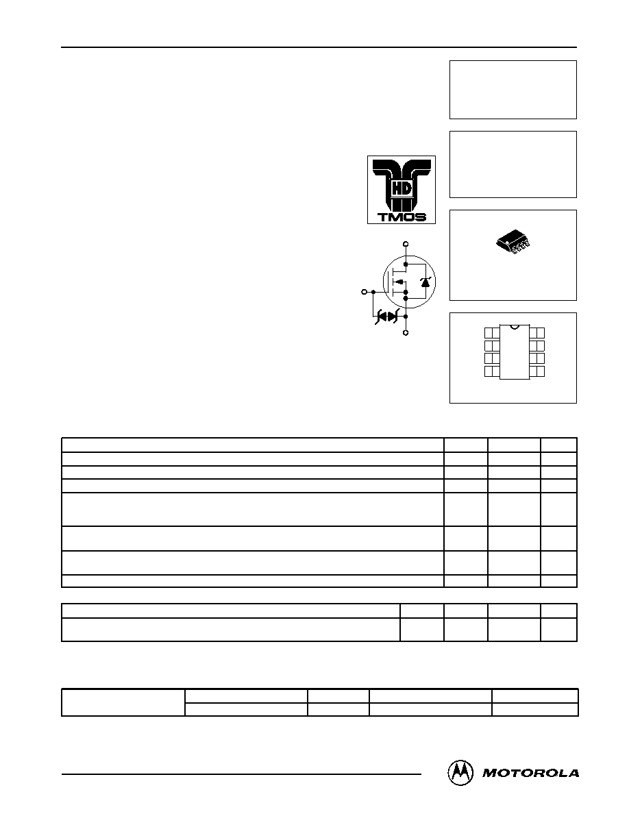
CASE 751–05, Style 11
SO–8
MMDF7N02Z
DUAL TMOS
POWER MOSFET
7.0 AMPERES
20 VOLTS
RDS(on) = 27 mW
Motorola Preferred Device
相关PDF资料 |
PDF描述 |
|---|---|
| MMDJ3N03BJTR2 | 3 A, 30 V, 2 CHANNEL, NPN, Si, POWER TRANSISTOR |
| MMDJ3N03BJT | 3 A, 30 V, 2 CHANNEL, NPN, Si, POWER TRANSISTOR |
| MMDJ3P03BJTR2 | 3 A, 30 V, 2 CHANNEL, PNP, Si, POWER TRANSISTOR |
| MMDJ3P03BJT | 3 A, 30 V, 2 CHANNEL, PNP, Si, POWER TRANSISTOR |
| MMDL101T1 | SILICON, VHF-UHF BAND, MIXER DIODE |
相关代理商/技术参数 |
参数描述 |
|---|---|
| MMDFS2P102 | 制造商:MOTOROLA 制造商全称:Motorola, Inc 功能描述:P-Channel Power MOSFET with Schottky Rectifier 20 Volts |
| MMDFS2P102R2 | 制造商:Rochester Electronics LLC 功能描述:- Bulk 制造商:ON Semiconductor 功能描述: |
| MMDFS3P303 | 制造商:ONSEMI 制造商全称:ON Semiconductor 功能描述:Power MOSFET 3 Amps, 30 Volts |
| MMDFS3P303-D | 制造商:ONSEMI 制造商全称:ON Semiconductor 功能描述:Power MOSFET 3 Amps, 30 Volts |
| MMDFS3P303R2 | 制造商:Rochester Electronics LLC 功能描述:- Bulk |
发布紧急采购,3分钟左右您将得到回复。