- 您现在的位置:买卖IC网 > PDF目录95979 > MMFT3055VLT1 (ON SEMICONDUCTOR) 1500 mA, 60 V, N-CHANNEL, Si, SMALL SIGNAL, MOSFET, TO-261AA PDF资料下载
参数资料
| 型号: | MMFT3055VLT1 |
| 厂商: | ON SEMICONDUCTOR |
| 元件分类: | 小信号晶体管 |
| 英文描述: | 1500 mA, 60 V, N-CHANNEL, Si, SMALL SIGNAL, MOSFET, TO-261AA |
| 封装: | CASE 318E-04, 4 PIN |
| 文件页数: | 6/10页 |
| 文件大小: | 219K |
| 代理商: | MMFT3055VLT1 |
MMFT3055VL
http://onsemi.com
5
VDS
,DRAINT
OSOURCE
VOL
TAGE
(VOL
TS)
V GS
,GA
TETOSOURCE
VOL
TAGE
(VOL
TS)
DRAINTOSOURCE DIODE CHARACTERISTICS
0.6 0.625
0.675
0.775
VSD, SOURCETODRAIN VOLTAGE (VOLTS)
Figure 8. GateToSource and DrainToSource
Voltage versus Total Charge
I S
,SOURCE
CURRENT
(AMPS)
Figure 9. Resistive Switching Time
Variation versus Gate Resistance
RG, GATE RESISTANCE (OHMS)
1
10
100
t,TIME
(ns)
VDD = 30 V
ID = 1.5 A
VGS = 5 V
TJ = 25°C
tf
td(off)
VGS = 0 V
TJ = 25°C
0
QT, TOTAL CHARGE (nC)
23
4
5
ID = 1.5 A
TJ = 25°C
VGS
0
1.2
1.6
1000
100
10
1
10
6
2
0
1
8
4
30
27
24
21
18
15
0
VDS
6
0.8
0.65
0.7 0.725
0.4
0.75
QT
Q1
Q2
Q3
7
1
td(on)
tr
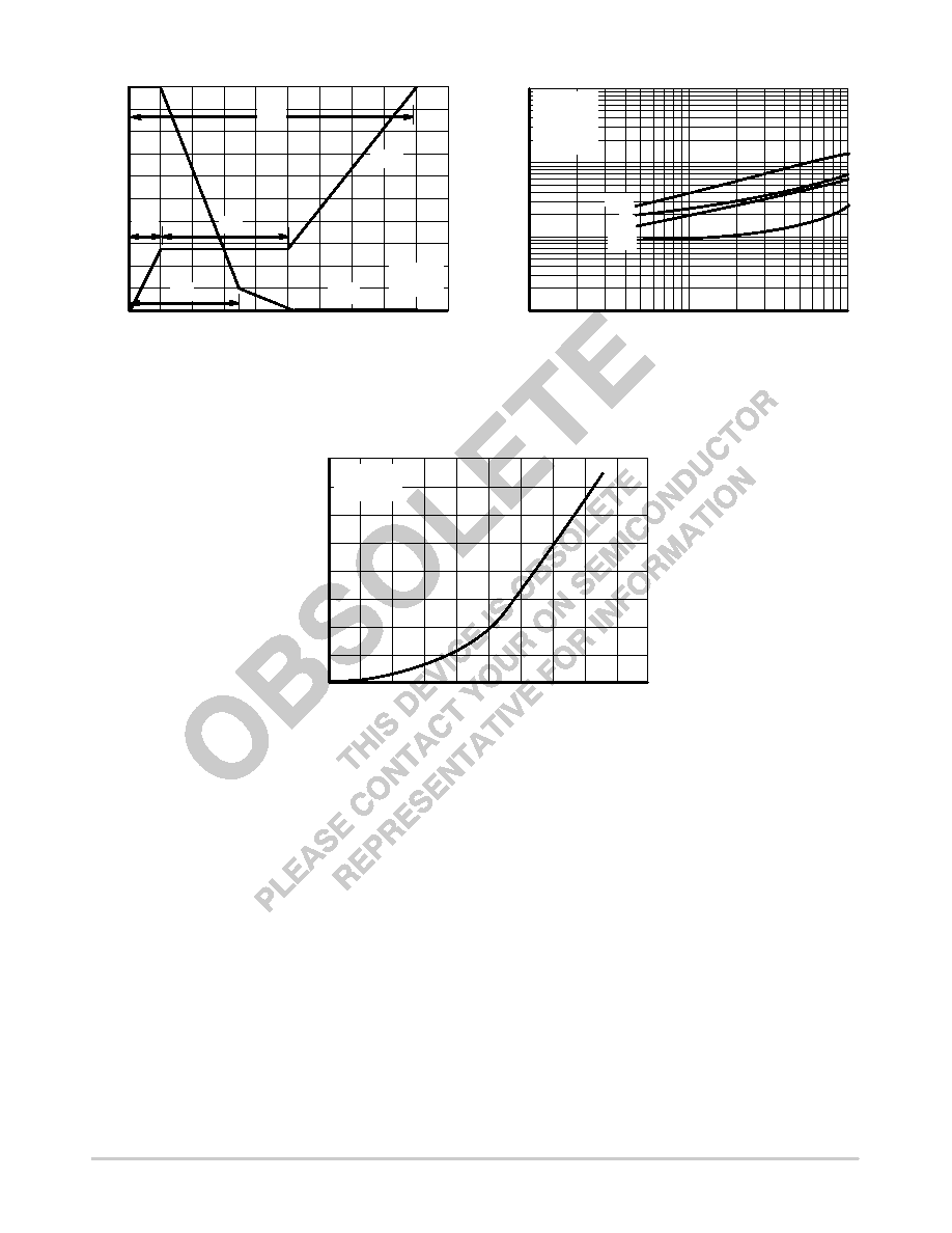
Figure 10. Diode Forward Voltage versus Current
7
3
9
5
12
3
6
9
1
1.4
0.6
0.2
0.8
89
10
0.825 0.85
SAFE OPERATING AREA
The Forward Biased Safe Operating Area curves define
the maximum simultaneous draintosource voltage and
drain current that a transistor can handle safely when it is
forward biased. Curves are based upon maximum peak
junction temperature and a case temperature (TC) of 25°C.
Peak repetitive pulsed power limits are determined by using
the thermal response data in conjunction with the procedures
discussed
in
AN569,
“Transient
Thermal
ResistanceGeneral Data and Its Use.”
Switching between the offstate and the onstate may
traverse any load line provided neither rated peak current
(IDM) nor rated voltage (VDSS) is exceeded and the
transition time (tr,tf) do not exceed 10 μs. In addition the total
power averaged over a complete switching cycle must not
exceed (TJ(MAX) TC)/(RθJC).
A Power MOSFET designated EFET can be safely used
in switching circuits with unclamped inductive loads. For
reliable operation, the stored energy from circuit inductance
dissipated in the transistor while in avalanche must be less
than the rated limit and adjusted for operating conditions
differing from those specified. Although industry practice is
to rate in terms of energy, avalanche energy capability is not
a constant. The energy rating decreases nonlinearly with an
increase of peak current in avalanche and peak junction
temperature.
Although many EFETs can withstand the stress of
draintosource avalanche at currents up to rated pulsed
current (IDM), the energy rating is specified at rated
continuous current (ID), in accordance with industry
custom. The energy rating must be derated for temperature
as shown in the accompanying graph (Figure 13). Maximum
energy at currents below rated continuous ID can safely be
assumed to equal the values indicated.
相关PDF资料 |
PDF描述 |
|---|---|
| MMFT3055VLT3 | 1500 mA, 60 V, N-CHANNEL, Si, SMALL SIGNAL, MOSFET, TO-261AA |
| MMFT3055VLT1 | 1500 mA, 60 V, N-CHANNEL, Si, SMALL SIGNAL, MOSFET, TO-261AA |
| MMFT3055VT1G | 1700 mA, 60 V, N-CHANNEL, Si, SMALL SIGNAL, MOSFET, TO-261AA |
| MMFT3055VT1 | 1700 mA, 60 V, N-CHANNEL, Si, SMALL SIGNAL, MOSFET, TO-261AA |
| MMFT3055VT1 | 1700 mA, 60 V, N-CHANNEL, Si, SMALL SIGNAL, MOSFET, TO-261AA |
相关代理商/技术参数 |
参数描述 |
|---|---|
| MMFT3055VT1 | 制造商:ON Semiconductor 功能描述:Trans MOSFET N-CH 60V 1.7A 4-Pin(3+Tab) SOT-223 T/R |
| MMFT3055VT3 | 制造商:ON Semiconductor 功能描述:Trans MOSFET N-CH 60V 1.7A 4-Pin(3+Tab) SOT-223 T/R |
| MMFT5P03HD | 制造商:MOTOROLA 制造商全称:Motorola, Inc 功能描述:TMOS MEDIUM POWER FET 5.2 AMPERES 30 VOLTS |
| MMFT5P03HDT1 | 功能描述:MOSFET P-CH 30V 3.7A SOT223 RoHS:否 类别:分离式半导体产品 >> FET - 单 系列:- 标准包装:1,000 系列:MESH OVERLAY™ FET 型:MOSFET N 通道,金属氧化物 FET 特点:逻辑电平门 漏极至源极电压(Vdss):200V 电流 - 连续漏极(Id) @ 25° C:18A 开态Rds(最大)@ Id, Vgs @ 25° C:180 毫欧 @ 9A,10V Id 时的 Vgs(th)(最大):4V @ 250µA 闸电荷(Qg) @ Vgs:72nC @ 10V 输入电容 (Ciss) @ Vds:1560pF @ 25V 功率 - 最大:40W 安装类型:通孔 封装/外壳:TO-220-3 整包 供应商设备封装:TO-220FP 包装:管件 |
| MMFT5P03HDT3 | 制造商:MOTOROLA 制造商全称:Motorola, Inc 功能描述:TMOS P-CHANNEL FIELD FEECT TRANSISTOR |
发布紧急采购,3分钟左右您将得到回复。