- 您现在的位置:买卖IC网 > PDF目录95982 > MMSF3305R2 (MOTOROLA INC) 6 A, 30 V, 0.02 ohm, P-CHANNEL, Si, POWER, MOSFET PDF资料下载
参数资料
| 型号: | MMSF3305R2 |
| 厂商: | MOTOROLA INC |
| 元件分类: | JFETs |
| 英文描述: | 6 A, 30 V, 0.02 ohm, P-CHANNEL, Si, POWER, MOSFET |
| 封装: | SO-8 |
| 文件页数: | 1/10页 |
| 文件大小: | 207K |
| 代理商: | MMSF3305R2 |
1
Motorola TMOS Power MOSFET Transistor Device Data
Product Preview
Medium Power Surface Mount Products
TMOS Single P-Channel
Field Effect Transistors
WaveFET
devices are an advanced series of power MOSFETs
which utilize Motorola’s High Cell Density HDTMOS process. These
miniature surface mount MOSFETs feature ultra low RDS(on) and true
logic level performance. They are capable of withstanding high energy in
the avalanche and commutation modes and the drain–to–source diode
has a very low reverse recovery time. WaveFET
devices are designed
for use in low voltage, high speed switching applications where power
efficiency is important. Typical applications are dc–dc converters, and
power management in portable and battery powered products such as
computers, printers, cellular and cordless phones. They can also be
used for low voltage motor controls in mass storage products such as
disk drives and tape drives. The avalanche energy is specified to
eliminate the guesswork in designs where inductive loads are switched
and offer additional safety margin against unexpected voltage transients.
Ultra Low RDS(on) Provides Higher Efficiency and Extends Battery Life
Logic Level Gate Drive — Can Be Driven by Logic ICs
Miniature SO–8 Surface Mount Package — Saves Board Space
Diode Is Characterized for Use In Bridge Circuits
Diode Exhibits High Speed, With Soft Recovery
IDSS Specified at Elevated Temperature
Avalanche Energy Specified
Mounting Information for SO–8 Package Provided
MAXIMUM RATINGS (TJ = 25°C unless otherwise noted)
Negative sign for P–Channel devices omitted for clarity
Rating
Symbol
Max
Unit
Drain–to–Source Voltage
VDSS
30
V
Drain–to–Gate Voltage (RGS = 1.0 M)
VDGR
20
V
Gate–to–Source Voltage — Continuous
VGS
± 20
V
1 inch SQ.
FR–4 or G–10 PCB
10 seconds
Thermal Resistance — Junction to Ambient
Total Power Dissipation @ TA = 25°C
Linear Derating Factor
Drain Current — Continuous @ TA = 25°C
Continuous @ TA = 70°C
Pulsed Drain Current (1)
RTHJA
PD
ID
IDM
50
2.5
20
8.0
6.7
50
°C/W
Watts
mW/
°C
A
Minimum
FR–4 or G–10 PCB
10 seconds
Thermal Resistance — Junction to Ambient
Total Power Dissipation @ TA = 25°C
Linear Derating Factor
Drain Current — Continuous @ TA = 25°C
Continuous @ TA = 70°C
Pulsed Drain Current (1)
RTHJA
PD
ID
IDM
80
1.56
12.5
6.0
5.3
40
°C/W
Watts
mW/
°C
A
Operating and Storage Temperature Range
TJ, Tstg
– 55 to 150
°C
Single Pulse Drain–to–Source Avalanche Energy — Starting TJ = 25°C
(VDD = 30 Vdc, VGS = 10 Vdc, Peak IL = 8.0 Apk, L = 47 mH, RG = 25 W)
EAS
1500
mJ
(1) Repetitive rating; pulse width limited by maximum junction temperature.
DEVICE MARKING
ORDERING INFORMATION
S3305
Device
Reel Size
Tape Width
Quantity
S3305
MMSF3305R2
13
″
12 mm embossed tape
4000 units
Preferred devices are Motorola recommended choices for future use and best overall value.
This document contains information on a product under development. Motorola reserves the right to change or discontinue this product without notice.
HDTMOS and WaveFET are trademarks of Motorola, Inc. TMOS is a registered trademark of Motorola, Inc.
REV 1
Order this document
by MMSF3305/D
MOTOROLA
SEMICONDUCTOR TECHNICAL DATA
Motorola, Inc. 1998
CASE 751–05, Style 13
SO–8
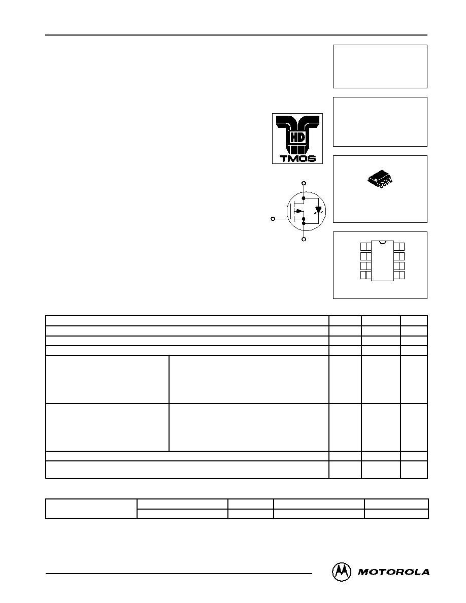
MMSF3305
SINGLE TMOS
POWER MOSFET
8 AMPERES
30 VOLTS
RDS(on) = 0.02 OHM
Motorola Preferred Device
Source
1
2
3
4
8
7
6
5
Top View
Source
Gate
Drain
D
S
G
相关PDF资料 |
PDF描述 |
|---|---|
| MMSF3P02HDR2 | 5.6 A, 20 V, 0.095 ohm, 2 CHANNEL, P-CHANNEL, Si, POWER, MOSFET |
| MMSF3P02ZR2 | 6500 mA, 20 V, P-CHANNEL, Si, SMALL SIGNAL, MOSFET |
| MMSF3P02ZR1 | 6500 mA, 20 V, P-CHANNEL, Si, SMALL SIGNAL, MOSFET |
| MMSF3P03HDR1 | 4600 mA, 30 V, P-CHANNEL, Si, SMALL SIGNAL, MOSFET |
| MMSF3P03HDR1 | 4600 mA, 30 V, P-CHANNEL, Si, SMALL SIGNAL, MOSFET |
相关代理商/技术参数 |
参数描述 |
|---|---|
| MMSF3350R2 | 制造商:Rochester Electronics LLC 功能描述:- Bulk |
| MMSF3P02HD | 制造商:MOTOROLA 制造商全称:Motorola, Inc 功能描述:SINGLE TMOS POWER MOSFET 3.0 AMPERES 20 VOLTS |
| MMSF3P02HDR2 | 功能描述:MOSFET 20V 3A P-Channel RoHS:否 制造商:STMicroelectronics 晶体管极性:N-Channel 汲极/源极击穿电压:650 V 闸/源击穿电压:25 V 漏极连续电流:130 A 电阻汲极/源极 RDS(导通):0.014 Ohms 配置:Single 最大工作温度: 安装风格:Through Hole 封装 / 箱体:Max247 封装:Tube |
| MMSF3P02HDR2G | 功能描述:MOSFET PFET SO8S 20V 5.6A 75mOhm RoHS:否 制造商:STMicroelectronics 晶体管极性:N-Channel 汲极/源极击穿电压:650 V 闸/源击穿电压:25 V 漏极连续电流:130 A 电阻汲极/源极 RDS(导通):0.014 Ohms 配置:Single 最大工作温度: 安装风格:Through Hole 封装 / 箱体:Max247 封装:Tube |
| MMSF3P02HDR2SG | 功能描述:MOSFET P-CH 20V 5.6A 8-SOIC RoHS:是 类别:分离式半导体产品 >> FET - 单 系列:- 标准包装:1,000 系列:MESH OVERLAY™ FET 型:MOSFET N 通道,金属氧化物 FET 特点:逻辑电平门 漏极至源极电压(Vdss):200V 电流 - 连续漏极(Id) @ 25° C:18A 开态Rds(最大)@ Id, Vgs @ 25° C:180 毫欧 @ 9A,10V Id 时的 Vgs(th)(最大):4V @ 250µA 闸电荷(Qg) @ Vgs:72nC @ 10V 输入电容 (Ciss) @ Vds:1560pF @ 25V 功率 - 最大:40W 安装类型:通孔 封装/外壳:TO-220-3 整包 供应商设备封装:TO-220FP 包装:管件 |
发布紧急采购,3分钟左右您将得到回复。