- 您现在的位置:买卖IC网 > PDF目录4105 > MPC8271CVRTIEA (Freescale Semiconductor)IC MPU POWERQUICC II 516-PBGA PDF资料下载
参数资料
| 型号: | MPC8271CVRTIEA |
| 厂商: | Freescale Semiconductor |
| 文件页数: | 19/61页 |
| 文件大小: | 0K |
| 描述: | IC MPU POWERQUICC II 516-PBGA |
| 标准包装: | 40 |
| 系列: | MPC82xx |
| 处理器类型: | 32-位 MPC82xx PowerQUICC II |
| 速度: | 400MHz |
| 电压: | 1.5V |
| 安装类型: | 表面贴装 |
| 封装/外壳: | 516-BBGA |
| 供应商设备封装: | 516-FPBGA(27x27) |
| 包装: | 托盘 |
第1页第2页第3页第4页第5页第6页第7页第8页第9页第10页第11页第12页第13页第14页第15页第16页第17页第18页当前第19页第20页第21页第22页第23页第24页第25页第26页第27页第28页第29页第30页第31页第32页第33页第34页第35页第36页第37页第38页第39页第40页第41页第42页第43页第44页第45页第46页第47页第48页第49页第50页第51页第52页第53页第54页第55页第56页第57页第58页第59页第60页第61页
MPC8272 PowerQUICC II Family Hardware Specifications, Rev. 3
26
Freescale Semiconductor
AC Electrical Characteristics
NOTE
The UPM machine outputs change on the internal tick determined by the
memory controller programming; the AC specifications are relative to the
internal tick. Note that SDRAM and GPCM machine outputs change on
CLKin’s rising edge.
6.3
JTAG Timings
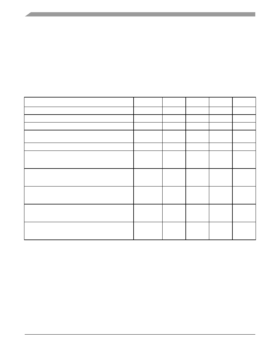
This table lists the JTAG timings.
Table 15. JTAG Timings1
Parameter
Symbol2
Min
Max
Unit
Notes
JTAG external clock frequency of operation
fJTG
033.3
MHz
—
JTAG external clock cycle time
tJTG
30
—
ns
—
JTAG external clock pulse width measured at 1.4V
tJTKHKL
15
—
ns
—
JTAG external clock rise and fall times
tJTGR and
tJTGF
05
ns
6
TRST assert time
tTRST
25
—
ns
3, 6
Input setup times
Boundary-scan data
TMS, TDI
tJTDVKH
tJTIVKH
4
—
ns
4, 7
Input hold times
Boundary-scan data
TMS, TDI
tJTDXKH
tJTIXKH
10
—
ns
4, 7
Output valid times
Boundary-scan data
TDO
tJTKLDV
tJTKLOV
—
10
ns
5, 7
5. 7
Output hold times
Boundary-scan data
TDO
tJTKLDX
tJTKLOX
1
—
ns
5, 7
JTAG external clock to output high impedance
Boundary-scan data
TDO
tJTKLDZ
tJTKLOZ
1
10
ns
5, 6
1 All outputs are measured from the midpoint voltage of the falling/rising edge of t
TCLK to the midpoint of the signal in question.
The output timings are measured at the pins. All output timings assume a purely resistive 50-
Ω load. Time-of-flight delays
must be added for trace lengths, vias, and connectors in the system.
2 The symbols used for timing specifications herein follow the pattern of t
(first two letters of functional block)(signal)(state) (reference)(state)
for inputs and t((first two letters of functional block)(reference)(state)(signal)(state) for outputs. For example, tJTDVKH symbolizes JTAG
device timing (JT) with respect to the time data input signals (D) reaching the valid state (V) relative to the tJTG clock reference
(K) going to the high (H) state or setup time. Also, tJTDXKH symbolizes JTAG timing (JT) with respect to the time data input
signals (D) went invalid (X) relative to the tJTG clock reference (K) going to the high (H) state. Note that, in general, the clock
reference symbol representation is based on three letters representing the clock of a particular functional. For rise and fall
times, the latter convention is used with the appropriate letter: R (rise) or F (fall).
3 TRST is an asynchronous level sensitive signal. The setup time is for test purposes only.
4 Non-JTAG signal input timing with respect to t
TCLK.
5 Non-JTAG signal output timing with respect to t
TCLK.
6 Guaranteed by design.
7 Guaranteed by design and device characterization.
相关PDF资料 |
PDF描述 |
|---|---|
| GSC60DTEN | CONN EDGECARD 120POS .100 EYELET |
| GSC60DTEH | CONN EDGECARD 120POS .100 EYELET |
| AMC40DRAN | CONN EDGECARD 80POS .100 R/A DIP |
| AMC40DRAH | CONN EDGECARD 80POS .100 R/A DIP |
| ACC65DRYS-S93 | CONN EDGECARD 130PS DIP .100 SLD |
相关代理商/技术参数 |
参数描述 |
|---|---|
| MPC8271CZQ | 制造商:MOTOROLA 制造商全称:Motorola, Inc 功能描述:MPC8272 PowerQUICC II Family Hardware Specifications |
| MPC8271CZQB | 制造商:FREESCALE 制造商全称:Freescale Semiconductor, Inc 功能描述:PowerQUICC II⑩ Family Hardware Specifications |
| MPC8271CZQE | 制造商:FREESCALE 制造商全称:Freescale Semiconductor, Inc 功能描述:PowerQUICC II⑩ Family Hardware Specifications |
| MPC8271CZQI | 制造商:FREESCALE 制造商全称:Freescale Semiconductor, Inc 功能描述:PowerQUICC II⑩ Family Hardware Specifications |
| MPC8271CZQM | 制造商:FREESCALE 制造商全称:Freescale Semiconductor, Inc 功能描述:PowerQUICC II⑩ Family Hardware Specifications |
发布紧急采购,3分钟左右您将得到回复。