- 您现在的位置:买卖IC网 > PDF目录80517 > MPC8309VMADDCA (FREESCALE SEMICONDUCTOR INC) 32-BIT, 266 MHz, RISC PROCESSOR, PBGA489 PDF资料下载
参数资料
| 型号: | MPC8309VMADDCA |
| 厂商: | FREESCALE SEMICONDUCTOR INC |
| 元件分类: | 微控制器/微处理器 |
| 英文描述: | 32-BIT, 266 MHz, RISC PROCESSOR, PBGA489 |
| 封装: | 19 X 19 MM, 1.61 MM HEIGHT, 0.80 MM PITCH, LEAD FREE, PLASTIC, MAPBGA-489 |
| 文件页数: | 2/81页 |
| 文件大小: | 484K |
| 代理商: | MPC8309VMADDCA |
第1页当前第2页第3页第4页第5页第6页第7页第8页第9页第10页第11页第12页第13页第14页第15页第16页第17页第18页第19页第20页第21页第22页第23页第24页第25页第26页第27页第28页第29页第30页第31页第32页第33页第34页第35页第36页第37页第38页第39页第40页第41页第42页第43页第44页第45页第46页第47页第48页第49页第50页第51页第52页第53页第54页第55页第56页第57页第58页第59页第60页第61页第62页第63页第64页第65页第66页第67页第68页第69页第70页第71页第72页第73页第74页第75页第76页第77页第78页第79页第80页第81页
MPC8309 PowerQUICC II Pro Integrated Communications Processor Family Hardware Specifications, Rev. 1
10
Freescale Semiconductor
Electrical Characteristics
2.1.3
Output Driver Characteristics
The following table provides information on the characteristics of the output driver strengths.
2.1.4
Input Capacitance Specification
The following table describes the input capacitance for the SYS_CLK_IN pin in the MPC8309.
2.2
Power Sequencing
The device does not require the core supply voltage (VDD) and IO supply voltages (GVDD and OVDD) to
be applied in any particular order. Note that during power ramp-up, before the power supplies are stable
and if the I/O voltages are supplied before the core voltage, there might be a period of time that all input
and output pins are actively driven and cause contention and excessive current. In order to avoid actively
driving the I/O pins and to eliminate excessive current draw, apply the core voltage (VDD) before the I/O
voltage (GVDD and OVDD) and assert PORESET before the power supplies fully ramp up. In the case
where the core voltage is applied first, the core voltage supply must rise to 90% of its nominal value before
the I/O supplies reach 0.7 V; see Figure 3. Once both the power supplies (I/O voltage and core voltage) are
stable, wait for a minimum of 32 clock cycles before negating PORESET.
NOTE
There is no specific power down sequence requirement for the device. I/O
voltage supplies (GVDD and OVDD) do not have any ordering requirements
with respect to one another.
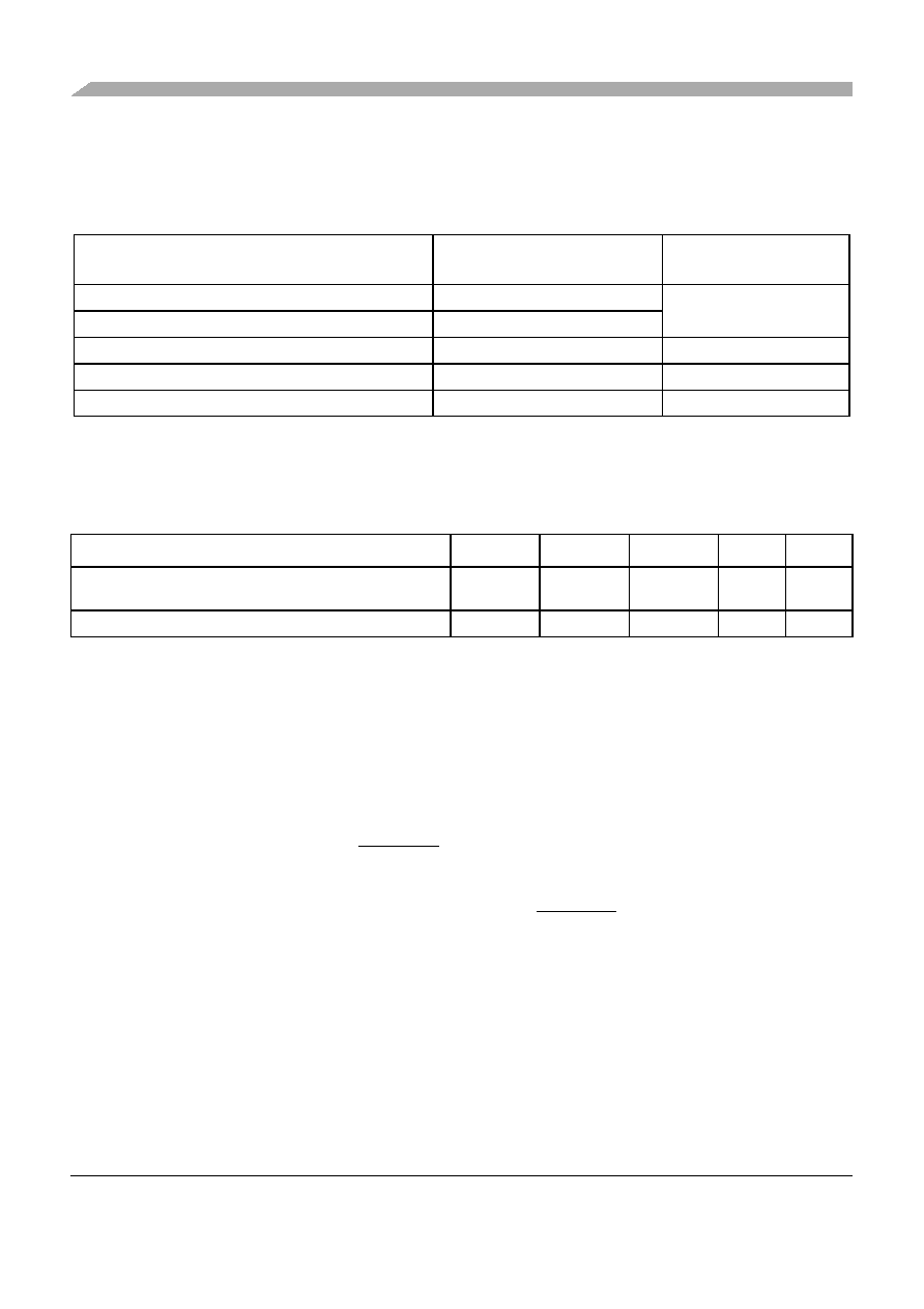
Table 3. Output Drive Capability
Driver Type
Output Impedance
(
)
Supply Voltage (V)
Local bus interface utilities signals
42
OVDD =3.3
PCI Signal
25
DDR2 signal
18
GVDD =1.8
DUART, system control, I2C, SPI, JTAG
42
OVDD =3.3
GPIO signals
42
OVDD =3.3
Table 4. Input Capacitance Specification
Parameter/Condition
Symbol
Min
Max
Unit
Note
Input capacitance for all pins except SYS_CLK_IN and
QE_CLK_IN
CI
68
pF
—
Input capacitance for SYS_CLK_IN and QE_CLK_IN
CICLK_IN
10
—
pF
1
Note:
1. The external clock generator should be able to drive 10 pF.
相关PDF资料 |
PDF描述 |
|---|---|
| MCF51JU128VHX | FLASH, 50 MHz, MICROCONTROLLER, QCC64 |
| MPC5601PEF0VLL4R | 32-BIT, FLASH, 64 MHz, RISC MICROCONTROLLER, PQFP100 |
| MB9BF105NAPMC | 32-BIT, FLASH, 80 MHz, RISC MICROCONTROLLER, PQFP100 |
| MB95F352EPF-G-SNE2 | 8-BIT, FLASH, 16.25 MHz, MICROCONTROLLER, PDSO24 |
| MB95F353LPFT-G-SNE2 | 8-BIT, FLASH, 16.25 MHz, MICROCONTROLLER, PDSO24 |
相关代理商/技术参数 |
参数描述 |
|---|---|
| MPC8309VMAFDC | 制造商:Freescale Semiconductor 功能描述:MPC8309VMAFDC - Bulk |
| MPC8309VMAFDCA | 功能描述:微处理器 - MPU E300 MP 333 RoHS:否 制造商:Atmel 处理器系列:SAMA5D31 核心:ARM Cortex A5 数据总线宽度:32 bit 最大时钟频率:536 MHz 程序存储器大小:32 KB 数据 RAM 大小:128 KB 接口类型:CAN, Ethernet, LIN, SPI,TWI, UART, USB 工作电源电压:1.8 V to 3.3 V 最大工作温度:+ 85 C 安装风格:SMD/SMT 封装 / 箱体:FBGA-324 |
| MPC8309VMAGDCA | 功能描述:微处理器 - MPU E300 MP 400 RoHS:否 制造商:Atmel 处理器系列:SAMA5D31 核心:ARM Cortex A5 数据总线宽度:32 bit 最大时钟频率:536 MHz 程序存储器大小:32 KB 数据 RAM 大小:128 KB 接口类型:CAN, Ethernet, LIN, SPI,TWI, UART, USB 工作电源电压:1.8 V to 3.3 V 最大工作温度:+ 85 C 安装风格:SMD/SMT 封装 / 箱体:FBGA-324 |
| MPC8309VMAHFCA | 功能描述:微处理器 - MPU 417/333/233 MP std tmp RoHS:否 制造商:Atmel 处理器系列:SAMA5D31 核心:ARM Cortex A5 数据总线宽度:32 bit 最大时钟频率:536 MHz 程序存储器大小:32 KB 数据 RAM 大小:128 KB 接口类型:CAN, Ethernet, LIN, SPI,TWI, UART, USB 工作电源电压:1.8 V to 3.3 V 最大工作温度:+ 85 C 安装风格:SMD/SMT 封装 / 箱体:FBGA-324 |
| MPC830X-TLCD | 功能描述:显示模块 Brd Computer MPC830x RoHS:否 制造商:4D Systems 显示器类型:TFT-LCD 显示分辨率—像素: 显示面积:2.8 in 背光类型: 接口类型:Serial 工作电源电压:4.5 V to 5.5 V 工作电源电流: 最大工作温度:+ 70 C 尺寸: |
发布紧急采购,3分钟左右您将得到回复。