- 您现在的位置:买卖IC网 > PDF目录4078 > MPC8314EVRADDA (Freescale Semiconductor)MPU POWERQUICC II PRO 620-PBGA PDF资料下载
参数资料
| 型号: | MPC8314EVRADDA |
| 厂商: | Freescale Semiconductor |
| 文件页数: | 80/101页 |
| 文件大小: | 0K |
| 描述: | MPU POWERQUICC II PRO 620-PBGA |
| 标准包装: | 36 |
| 系列: | MPC83xx |
| 处理器类型: | 32-位 MPC83xx PowerQUICC II Pro |
| 速度: | 266MHz |
| 电压: | 1V |
| 安装类型: | 表面贴装 |
| 封装/外壳: | 620-BBGA 裸露焊盘 |
| 供应商设备封装: | 620-PBGA(29x29) |
| 包装: | 托盘 |
第1页第2页第3页第4页第5页第6页第7页第8页第9页第10页第11页第12页第13页第14页第15页第16页第17页第18页第19页第20页第21页第22页第23页第24页第25页第26页第27页第28页第29页第30页第31页第32页第33页第34页第35页第36页第37页第38页第39页第40页第41页第42页第43页第44页第45页第46页第47页第48页第49页第50页第51页第52页第53页第54页第55页第56页第57页第58页第59页第60页第61页第62页第63页第64页第65页第66页第67页第68页第69页第70页第71页第72页第73页第74页第75页第76页第77页第78页第79页当前第80页第81页第82页第83页第84页第85页第86页第87页第88页第89页第90页第91页第92页第93页第94页第95页第96页第97页第98页第99页第100页第101页
MPC8314E PowerQUICC II Pro Processor Hardware Specifications, Rev. 2
8
Freescale Semiconductor
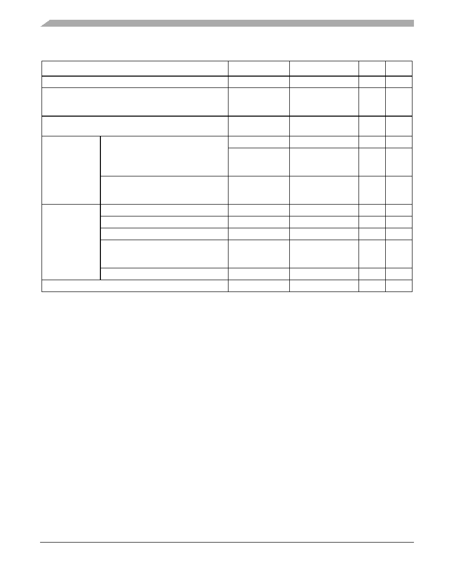
Electrical Characteristics
DDR2 DRAM I/O supply voltage
GVDD
–0.3 to 1.9
V
—
PCI, local bus, DUART, system control and power
management, I2C, Ethernet management, 1588 timer and
JTAG I/O voltage
NVDD
–0.3 to 3.6
V
7
USB, and eTSEC I/O voltage
LVDD
–0.3 to 2.75 or
–0.3 to 3.6
V6, 8
PHY voltage
USB PHY
USB_PLL_PWR1
–0.3 to 1.26
V
—
USB_PLL_PWR3,
USB_VDDA_BIAS,
VDDA
–0.3 to 3.6
V
—
SERDES PHY
XCOREVDD,
XPADVDD,
SDAVDD
–0.3 to 1.26
V
—
Input voltage
DDR DRAM signals
MVIN
–0.3 to (GVDD + 0.3)
V
2, 4
DDR DRAM reference
MVREF
–0.3 to (GVDD + 0.3)
V
2, 4
eTSEC signals
LVIN
–0.3 to (LVDD + 0.3)
V
3, 4
Local bus, DUART, SYS_CLK_IN, system
control and power management, I2C, and
JTAG signals
NVIN
–0.3 to (NVDD + 0.3)
V
3, 4
PCI
NVIN
–0.3 to (NVDD + 0.3)
V
5
Storage temperature range
TSTG
–55 to150
C—
Note:
1. Functional and tested operating conditions are given in Table 2. Absolute maximum ratings are stress ratings only, and
functional operation at the maximums is not guaranteed. Stresses beyond those listed may affect device reliability or cause
permanent damage to the device.
2. Caution: MVIN must not exceed GVDD by more than 0.3 V. This limit may be exceeded for a maximum of 20 ms during
power-on reset and power-down sequences.
3. Caution: (N,L)VIN must not exceed (N,L)VDD by more than 0.3 V. This limit may be exceeded for a maximum of 20 ms
during power-on reset and power-down sequences.
4. (M,N,L)VIN and MVREF may overshoot/undershoot to a voltage and for a maximum duration as shown in Figure 2.
5. NVIN on the PCI interface may overshoot/undershoot according to the PCI Electrical Specification for 3.3-V operation, as
shown in Figure 2.
6. The max value of supply voltage should be selected based on the RGMII mode.
7. NVDD means NVDD1_OFF, NVDD1_ON, NVDD2_OFF, NVDD2_ON, NVDD3_OFF, NVDD4_OFF
8. LVDD means LVDD1_OFF and LVDD2_ON
Table 1. Absolute Maximum Ratings 1 (continued)
Characteristic
Symbol
Max Value
Unit
Note
相关PDF资料 |
PDF描述 |
|---|---|
| MC68SEC000CAA20 | IC MPU 32BIT 20MHZ 64-QFP |
| IDT70V06S55PF8 | IC SRAM 128KBIT 55NS 64TQFP |
| MPC8321CZQADDC | IC MPU PWRQUICC II 516-PBGA |
| IDT7025S55PF8 | IC SRAM 128KBIT 55NS 100TQFP |
| IDT7006S55PF8 | IC SRAM 128KBIT 55NS 64TQFP |
相关代理商/技术参数 |
参数描述 |
|---|---|
| MPC8314EVRAFDA | 功能描述:微处理器 - MPU ENCRYPT RoHS:否 制造商:Atmel 处理器系列:SAMA5D31 核心:ARM Cortex A5 数据总线宽度:32 bit 最大时钟频率:536 MHz 程序存储器大小:32 KB 数据 RAM 大小:128 KB 接口类型:CAN, Ethernet, LIN, SPI,TWI, UART, USB 工作电源电压:1.8 V to 3.3 V 最大工作温度:+ 85 C 安装风格:SMD/SMT 封装 / 箱体:FBGA-324 |
| MPC8314EVRAGDA | 功能描述:微处理器 - MPU ENCRYPT RoHS:否 制造商:Atmel 处理器系列:SAMA5D31 核心:ARM Cortex A5 数据总线宽度:32 bit 最大时钟频率:536 MHz 程序存储器大小:32 KB 数据 RAM 大小:128 KB 接口类型:CAN, Ethernet, LIN, SPI,TWI, UART, USB 工作电源电压:1.8 V to 3.3 V 最大工作温度:+ 85 C 安装风格:SMD/SMT 封装 / 箱体:FBGA-324 |
| MPC8314VRADDA | 功能描述:微处理器 - MPU NON-ENCRYPT RoHS:否 制造商:Atmel 处理器系列:SAMA5D31 核心:ARM Cortex A5 数据总线宽度:32 bit 最大时钟频率:536 MHz 程序存储器大小:32 KB 数据 RAM 大小:128 KB 接口类型:CAN, Ethernet, LIN, SPI,TWI, UART, USB 工作电源电压:1.8 V to 3.3 V 最大工作温度:+ 85 C 安装风格:SMD/SMT 封装 / 箱体:FBGA-324 |
| MPC8314VRAFDA | 功能描述:微处理器 - MPU NON-ENCRYPT RoHS:否 制造商:Atmel 处理器系列:SAMA5D31 核心:ARM Cortex A5 数据总线宽度:32 bit 最大时钟频率:536 MHz 程序存储器大小:32 KB 数据 RAM 大小:128 KB 接口类型:CAN, Ethernet, LIN, SPI,TWI, UART, USB 工作电源电压:1.8 V to 3.3 V 最大工作温度:+ 85 C 安装风格:SMD/SMT 封装 / 箱体:FBGA-324 |
| MPC8314VRAGDA | 功能描述:微处理器 - MPU NON-ENCRYPT RoHS:否 制造商:Atmel 处理器系列:SAMA5D31 核心:ARM Cortex A5 数据总线宽度:32 bit 最大时钟频率:536 MHz 程序存储器大小:32 KB 数据 RAM 大小:128 KB 接口类型:CAN, Ethernet, LIN, SPI,TWI, UART, USB 工作电源电压:1.8 V to 3.3 V 最大工作温度:+ 85 C 安装风格:SMD/SMT 封装 / 箱体:FBGA-324 |
发布紧急采购,3分钟左右您将得到回复。