- 您现在的位置:买卖IC网 > PDF目录80377 > MPC8323ZQAFDCA (FREESCALE SEMICONDUCTOR INC) 32-BIT, 333 MHz, RISC PROCESSOR, PBGA516 PDF资料下载
参数资料
| 型号: | MPC8323ZQAFDCA |
| 厂商: | FREESCALE SEMICONDUCTOR INC |
| 元件分类: | 微控制器/微处理器 |
| 英文描述: | 32-BIT, 333 MHz, RISC PROCESSOR, PBGA516 |
| 封装: | 27 X 27 MM, 2.25 MM HEIGHT, 1 MM PITCH, PLASTIC, PBGA-516 |
| 文件页数: | 3/82页 |
| 文件大小: | 1134K |
| 代理商: | MPC8323ZQAFDCA |
第1页第2页当前第3页第4页第5页第6页第7页第8页第9页第10页第11页第12页第13页第14页第15页第16页第17页第18页第19页第20页第21页第22页第23页第24页第25页第26页第27页第28页第29页第30页第31页第32页第33页第34页第35页第36页第37页第38页第39页第40页第41页第42页第43页第44页第45页第46页第47页第48页第49页第50页第51页第52页第53页第54页第55页第56页第57页第58页第59页第60页第61页第62页第63页第64页第65页第66页第67页第68页第69页第70页第71页第72页第73页第74页第75页第76页第77页第78页第79页第80页第81页第82页
MPC8323E PowerQUICC II Pro Integrated Communications Processor Family Hardware Specifications, Rev. 4
Freescale Semiconductor
11
RESET Initialization
4.2
AC Electrical Characteristics
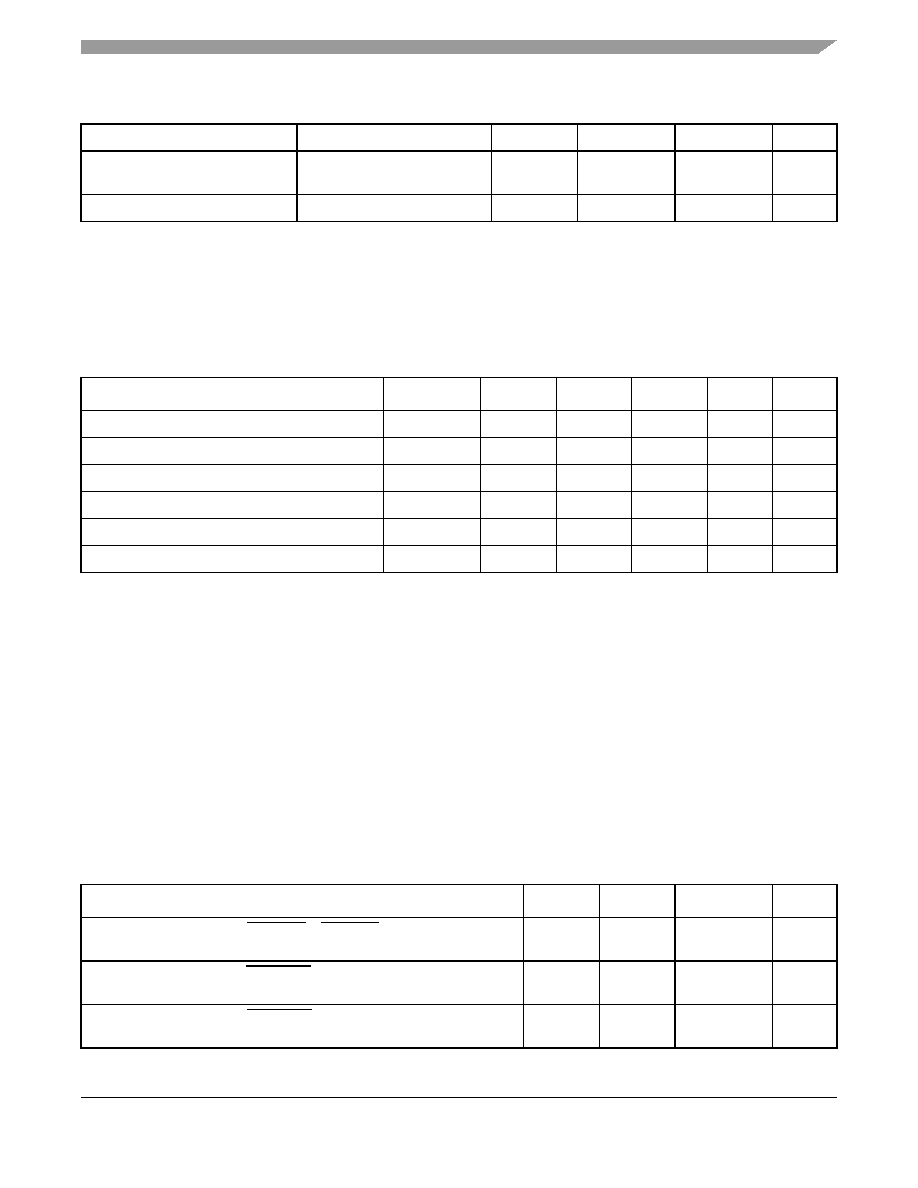
The primary clock source for the MPC8323E can be one of two inputs, CLKIN or PCI_CLK, depending
on whether the device is configured in PCI host or PCI agent mode. Table 8 provides the clock input
(CLKIN/PCI_CLK) AC timing specifications for the MPC8323E.
5
RESET Initialization
This section describes the AC electrical specifications for the reset initialization timing requirements of
the MPC8323E. Table 9 provides the reset initialization AC timing specifications for the reset
component(s).
CLKIN input current
0 V
≤ VIN ≤ OVDD
IIN
—±5
μA
PCI_SYNC_IN input current
0 V
≤ VIN ≤ 0.5 V or
OVDD – 0.5 V ≤ VIN ≤ OVDD
IIN
—±5
μA
PCI_SYNC_IN input current
0.5 V
≤ VIN ≤ OVDD – 0.5 V
IIN
—±50
μA
Table 8. CLKIN AC Timing Specifications
Parameter/Condition
Symbol
Min
Typical
Max
Unit
Notes
CLKIN/PCI_CLK frequency
fCLKIN
25
—
66.67
MHz
1
CLKIN/PCI_CLK cycle time
tCLKIN
15
—
ns
—
CLKIN rise and fall time
tKH, tKL
0.6
0.8
4
ns
2
PCI_CLK rise and fall time
tPCH, tPCL
0.6
0.8
1.2
ns
2
CLKIN/PCI_CLK duty cycle
tKHK/tCLKIN
40
—
60
%
3
CLKIN/PCI_CLK jitter
—
±150
ps
4, 5
Notes:
1. Caution: The system, core, security, and QUICC Engine block must not exceed their respective maximum or minimum
operating frequencies.
2. Rise and fall times for CLKIN/PCI_CLK are measured at 0.4 and 2.7 V.
3. Timing is guaranteed by design and characterization.
4. This represents the total input jitter—short term and long term—and is guaranteed by design.
5. The CLKIN/PCI_CLK driver’s closed loop jitter bandwidth should be < 500 kHz at –20 dB. The bandwidth must be set low to
allow cascade-connected PLL-based devices to track CLKIN drivers with the specified jitter.
Table 9. RESET Initialization Timing Specifications
Parameter/Condition
Min
Max
Unit
Notes
Required assertion time of HRESET or SRESET (input) to activate reset
flow
32
—
tPCI_SYNC_IN
1
Required assertion time of PORESET with stable clock applied to CLKIN
when the MPC8323E is in PCI host mode
32
—
tCLKIN
2
Required assertion time of PORESET with stable clock applied to
PCI_SYNC_IN when the MPC8323E is in PCI agent mode
32
—
tPCI_SYNC_IN
1
Table 7. CLKIN DC Electrical Characteristics (continued)
相关PDF资料 |
PDF描述 |
|---|---|
| MB90867ESPF | 16-BIT, MROM, 24 MHz, MICROCONTROLLER, PQFP100 |
| MB96F346AWAXXXPQC-GSE2 | 16-BIT, FLASH, 56 MHz, RISC MICROCONTROLLER, PQFP100 |
| MB96F348HWBXXXPQC-GSE2 | 16-BIT, FLASH, 56 MHz, RISC MICROCONTROLLER, PQFP100 |
| M37478E8FP | 8-BIT, OTPROM, 8 MHz, MICROCONTROLLER, PQFP56 |
| MB90342CEPFV | MICROCONTROLLER, PQFP100 |
相关代理商/技术参数 |
参数描述 |
|---|---|
| MPC832XE-MDS-PB | 功能描述:开发板和工具包 - 其他处理器 PROCESSOR BOARD (SOCKET) RoHS:否 制造商:Freescale Semiconductor 产品:Development Systems 工具用于评估:P3041 核心:e500mc 接口类型:I2C, SPI, USB 工作电源电压: |
| MPC8343CVRADD | 功能描述:IC MPU PWRQUICC II PRO 620-PBGA RoHS:是 类别:集成电路 (IC) >> 嵌入式 - 微处理器 系列:MPC83xx 标准包装:1 系列:MPC85xx 处理器类型:32-位 MPC85xx PowerQUICC III 特点:- 速度:1.2GHz 电压:1.1V 安装类型:表面贴装 封装/外壳:783-BBGA,FCBGA 供应商设备封装:783-FCPBGA(29x29) 包装:托盘 |
| MPC8343CVRADDB | 功能描述:微处理器 - MPU 8347 PBGA NO-PB W/O ENCR RoHS:否 制造商:Atmel 处理器系列:SAMA5D31 核心:ARM Cortex A5 数据总线宽度:32 bit 最大时钟频率:536 MHz 程序存储器大小:32 KB 数据 RAM 大小:128 KB 接口类型:CAN, Ethernet, LIN, SPI,TWI, UART, USB 工作电源电压:1.8 V to 3.3 V 最大工作温度:+ 85 C 安装风格:SMD/SMT 封装 / 箱体:FBGA-324 |
| MPC8343CVRAGD | 功能描述:IC MPU PWRQUICC II PRO 620-PBGA RoHS:是 类别:集成电路 (IC) >> 嵌入式 - 微处理器 系列:MPC83xx 标准包装:1 系列:MPC85xx 处理器类型:32-位 MPC85xx PowerQUICC III 特点:- 速度:1.2GHz 电压:1.1V 安装类型:表面贴装 封装/外壳:783-BBGA,FCBGA 供应商设备封装:783-FCPBGA(29x29) 包装:托盘 |
| MPC8343CVRAGDB | 功能描述:微处理器 - MPU 8347 PBGA NO-PB W/O ENCR RoHS:否 制造商:Atmel 处理器系列:SAMA5D31 核心:ARM Cortex A5 数据总线宽度:32 bit 最大时钟频率:536 MHz 程序存储器大小:32 KB 数据 RAM 大小:128 KB 接口类型:CAN, Ethernet, LIN, SPI,TWI, UART, USB 工作电源电压:1.8 V to 3.3 V 最大工作温度:+ 85 C 安装风格:SMD/SMT 封装 / 箱体:FBGA-324 |
发布紧急采购,3分钟左右您将得到回复。