- 您现在的位置:买卖IC网 > Datasheet目录344 > MPC8349E-MITXE (Freescale Semiconductor)BOARD REFERENCE FOR MPC8349 Datasheet资料下载
参数资料
| 型号: | MPC8349E-MITXE |
| 厂商: | Freescale Semiconductor |
| 文件页数: | 12/48页 |
| 文件大小: | 0K |
| 描述: | BOARD REFERENCE FOR MPC8349 |
| 产品培训模块: | MPC834x PowerQUICC II Processors |
| 标准包装: | 1 |
| 系列: | PowerQUICC II™ PRO |
| 类型: | MPU |
| 适用于相关产品: | MPC8349E |
| 所含物品: | 模块和其他硬件 |
| 相关产品: | MPC8349ECZUAJFB-ND - IC MPU POWERQUICC II PRO 672TBGA MPC8349ECVVAJFB-ND - IC MPU POWERQUICC II PRO 672TBGA MPC8349CZUAJFB-ND - IC MPU POWERQUICC II PRO 672TBGA MPC8349CZUAJDB-ND - IC MPU POWERQUICC II PRO 672TBGA MPC8349CZUAGDB-ND - IC MPU POWERQUICC II PRO 672TBGA MPC8349CVVAJFB-ND - IC MPU POWERQUICC II PRO 672TBGA MPC8349CVVAJDB-ND - IC MPU POWERQUICC II PRO 672TBGA MPC8349CVVAGDB-ND - IC MPU POWERQUICC II 672TBGA MPC8349ZUAJDB-ND - IC MPU PWRQUICC II 672-TBGA MPC8349ZUAJFB-ND - IC MPU PWRQUICC II 672-TBGA 更多... |
| 其它名称: | MPC8349E-MITXE -ND |
第1页第2页第3页第4页第5页第6页第7页第8页第9页第10页第11页当前第12页第13页第14页第15页第16页第17页第18页第19页第20页第21页第22页第23页第24页第25页第26页第27页第28页第29页第30页第31页第32页第33页第34页第35页第36页第37页第38页第39页第40页第41页第42页第43页第44页第45页第46页第47页第48页
�� �
�
�MPC8349E-mITXE� Board�
�Table� 5.� PCF8574A� (U10)� Bit� Descriptions� (continued)�
�PCF8574A�
�(U10)� bit[0..7]�
�4�
�Name�
�MPCI_CLKRUN�
�Read/Write�
�Read/Write�
�Description�
�MiniPCI� clock� run� signal� level,� defined� by� the� PCI� Mobile� Design�
�Guide.�
�0:� MiniPCI� clock� is� in� normal� operating� frequency�
�1:� MiniPCI� clock� is� stopped� or� running� very� low�
�5�
�PCI_M66EN�
�Read� only,� write�
�has� no� effect�
�PCI� M66EN� Signal�
�0:� PCI� M66EN� signal� is� low,� indicates� the� PCI� cards� on� PCI� slot� and�
�miniPCI� slot� are� not� 66� MHz� capable�
�1:� PCI� M66EN� signal� is� high,� indicates� the� PCI� cards� on� PCI� slot� and�
�miniPCI� slot� are� 66� MHz� capable�
�6�
�BOOT0�
�Read� only,� write�
�has� no� effect�
�Used� to� determine� which� Flash� is� used� for� boot� Flash�
�0:� Flash� 0� (U4)� is� the� boot� Flash�
�1:� Flash� 1� (U7)� is� the� boot� Flash�
�7�
�Not� used�
�—�
�—�
�The� DS1339� RTC� is� connected� to� I� 2� C� with� address� 0x68.� The� software� running� on� PowerPC� core� can� read�
�or� write� to� the� RTC� through� the� I2C2� interface.�
�1.2.8�
�Compact� Flash� Interface�
�A� compact� Flash� interface� connects� directly� to� the� local� bus� without� a� PCMCIA� controller.� The� true� IDE�
�mode� is� the� only� compact� Flash� operating� mode� supported� by� this� connection.� Hot� insertion� and� removal�
�is� not� supported.� The� MPC8349E� universal� programmable� machine� A� (UPMA)� is� used� to� generate� the�
�required� timing� for� IORD� and� IOWR� through� the� LGPL0� and� LGPL1� signals.�
�The� true� IDE� mode� requires� three� address� signals� (A[0:2])� and� two� chip-enable� signals� (CE[1:2])� to�
�address� the� 10� registers� in� the� AT� task� file.� Therefore,� glue� logic� is� used� to� split� CS3� into� two� regions.� One�
�chip-select� signal� (CS3)� is� assigned� to� the� compact� Flash� interface.� Glue� logic� is� used� to� generate� the� CE1�
�and� CE2� signals� required� by� the� compact� Flash.� The� logic� simply� uses� the� local� bus� address� A22� to�
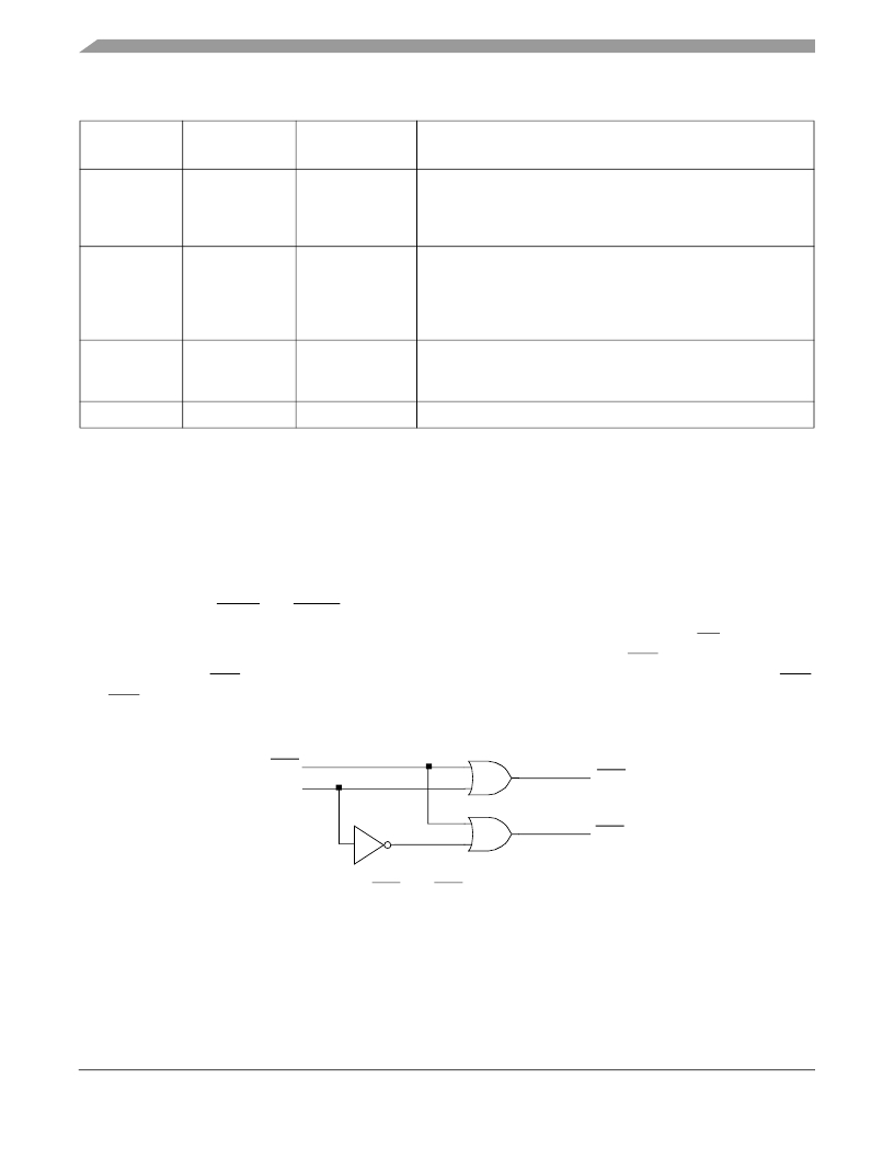
��CS3�
�LBA22�
�CE1�
�CE2�
�Figure� 7.� CE1� and� CE2� Generation� Logic�
�MPC8349E-mITXE� Reference� Design� Platform� User’s� Guide,� Rev.� 2�
�12�
�Preliminary—Subject� to� Change� Without� Notice�
�Freescale� Semiconductor�
�相关PDF资料 |
PDF描述 |
|---|---|
| MPC8377E-MDS-PB | BOARD MODULAR DEV SYSTEM |
| MPC8569E-MDS-PB | BOARD MOD DEV SYSTEM MPC8569 |
| MPC8572EAMC | MPC8572 AMC RAPID SYSTEM |
| MPQ-ARM | ISP 4PORT FOR ARM CORTEX MCU |
| MP | SURGE SUPPRESSR 2/RJ11 MODEM/FAX |
相关代理商/技术参数 |
参数描述 |
|---|---|
| MPC8349E-MITXE | 制造商:Freescale Semiconductor 功能描述:MPC8349E Reference Platform |
| MPC8349E-MITX-GP | 功能描述:开发板和工具包 - 其他处理器 GP REF DESGN BRD FOR MPC RoHS:否 制造商:Freescale Semiconductor 产品:Development Systems 工具用于评估:P3041 核心:e500mc 接口类型:I2C, SPI, USB 工作电源电压: |
| MPC8349E-MITX-GP | 制造商:Freescale Semiconductor 功能描述:MPC8349e-MITX-GP Industrial Re |
| MPC8349EVVAGD | 功能描述:IC MPU PWRQUICC II PRO 672-TBGA RoHS:是 类别:集成电路 (IC) >> 嵌入式 - 微处理器 系列:MPC83xx 标准包装:1 系列:MPC85xx 处理器类型:32-位 MPC85xx PowerQUICC III 特点:- 速度:1.2GHz 电压:1.1V 安装类型:表面贴装 封装/外壳:783-BBGA,FCBGA 供应商设备封装:783-FCPBGA(29x29) 包装:托盘 |
| MPC8349EVVAGDB | 功能描述:微处理器 - MPU 8349 TBGA NO PB W/ ENC RoHS:否 制造商:Atmel 处理器系列:SAMA5D31 核心:ARM Cortex A5 数据总线宽度:32 bit 最大时钟频率:536 MHz 程序存储器大小:32 KB 数据 RAM 大小:128 KB 接口类型:CAN, Ethernet, LIN, SPI,TWI, UART, USB 工作电源电压:1.8 V to 3.3 V 最大工作温度:+ 85 C 安装风格:SMD/SMT 封装 / 箱体:FBGA-324 |
发布紧急采购,3分钟左右您将得到回复。