- 您现在的位置:买卖IC网 > Datasheet目录344 > MPC8349E-MITXE (Freescale Semiconductor)BOARD REFERENCE FOR MPC8349 Datasheet资料下载
参数资料
| 型号: | MPC8349E-MITXE |
| 厂商: | Freescale Semiconductor |
| 文件页数: | 31/48页 |
| 文件大小: | 0K |
| 描述: | BOARD REFERENCE FOR MPC8349 |
| 产品培训模块: | MPC834x PowerQUICC II Processors |
| 标准包装: | 1 |
| 系列: | PowerQUICC II™ PRO |
| 类型: | MPU |
| 适用于相关产品: | MPC8349E |
| 所含物品: | 模块和其他硬件 |
| 相关产品: | MPC8349ECZUAJFB-ND - IC MPU POWERQUICC II PRO 672TBGA MPC8349ECVVAJFB-ND - IC MPU POWERQUICC II PRO 672TBGA MPC8349CZUAJFB-ND - IC MPU POWERQUICC II PRO 672TBGA MPC8349CZUAJDB-ND - IC MPU POWERQUICC II PRO 672TBGA MPC8349CZUAGDB-ND - IC MPU POWERQUICC II PRO 672TBGA MPC8349CVVAJFB-ND - IC MPU POWERQUICC II PRO 672TBGA MPC8349CVVAJDB-ND - IC MPU POWERQUICC II PRO 672TBGA MPC8349CVVAGDB-ND - IC MPU POWERQUICC II 672TBGA MPC8349ZUAJDB-ND - IC MPU PWRQUICC II 672-TBGA MPC8349ZUAJFB-ND - IC MPU PWRQUICC II 672-TBGA 更多... |
| 其它名称: | MPC8349E-MITXE -ND |
第1页第2页第3页第4页第5页第6页第7页第8页第9页第10页第11页第12页第13页第14页第15页第16页第17页第18页第19页第20页第21页第22页第23页第24页第25页第26页第27页第28页第29页第30页当前第31页第32页第33页第34页第35页第36页第37页第38页第39页第40页第41页第42页第43页第44页第45页第46页第47页第48页
�� �
�
�MPC8349E-mITXE� Board�
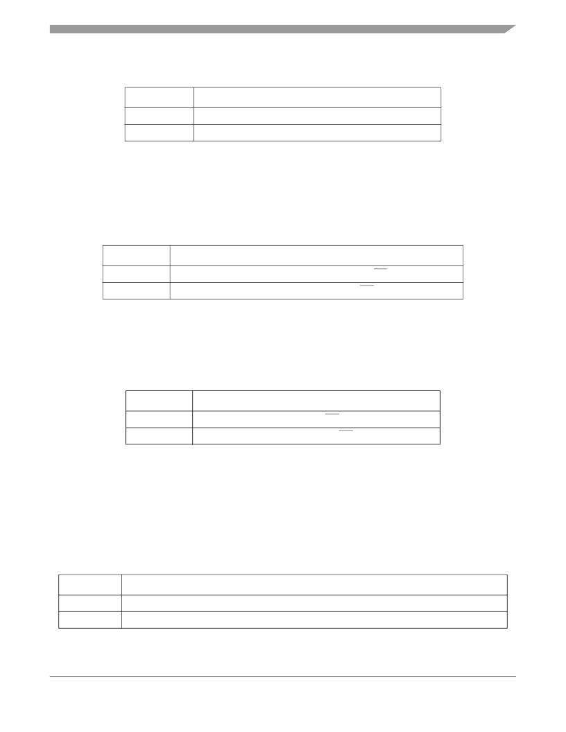
�Table� 15.� Flash� Bank� for� Booting� the� System�
�J22.E�
�Jumper� Off�
�Jumper� On�
�The� booting� bank� is� U4.�
�The� booting� bank� is� U7.�
�Description�
�The� two� Flash� memory� banks� are� MX29LV640MTTC-90� top� boot� Flash� memory� devices.� Each� Flash�
�memory� bank� has� 135� sectors.� The� first� 127� sectors,� SA[0–126],� are� 64� Kbyte,� and� the� last� 8� sectors,�
�SA[127–134],� are� 8� Kbyte.� These� last� 8� sectors� can� be� write-protected� to� prevent� accidental� erasure� of� the�
�sector� content� for� applications� that� may� choose� to� use� this� protection� feature.� Table� 16� shows� the� jumper�
�settings� to� write-protect� sectors� SA[127–134]� of� Flash� memory.�
�Table� 16.� Flash� Memory� Write� Protect� of� SA[127–134]�
�J22.H�
�Jumper� Off�
�Jumper� On�
�Description�
�Flash� (U4� and� U7)� top� sectors� are� not� write� protected� (WP� not� asserted).�
�Flash� (U4� and� U7)� top� sectors� are� write� protected� (WP� asserted).�
�1.6.2�
�EEPROM�
�An� on-board� serial� EEPROM� allows� storage� of� miscellaneous� board-related� data.� The� EEPROM� can� be�
��Table� 17.� EEPROM� Write� Protect�
�J22.G�
�Jumper� Off�
�Jumper� On�
�Description�
�Serial� EEPROM� is� write� protected� (WC� not� asserted).�
�Serial� EEPROM� is� not� write� protected� (WC� asserted).�
�1.6.3�
�PCI� Operating� Frequency�
�An� M66EN� input� pin� determines� the� AC� timing� of� the� PCI� interface.� On� the� MPC8349E-mITXE� board,�
�the� state� of� this� signal� can� be� driven� to� 0� by� the� J22� jumper� to� select� 33� MHz� AC� timing.� If� J22.F� is� not�
�driven� to� 0,� the� M66EN� signal� level� is� determined� by� the� PCI� agent� card� connected� to� PCI� slot� P1.� If� a� 33�
�MHz� only� card� is� inserted,� the� M66EN� signal� is� driven� to� 0� by� the� PCI� agent� card� according� to� the� PCI�
��.�
�Table� 18.� M66EN� Signal� Status� Selection�
�J22.F�
�Jumper� Off�
�Jumper� On�
�Description�
�M66EN� signal� is� determined� by� the� card� plugged� into� the� PCI� slot� (PCI� 32-bit� slot� and� MiniPCI� slot).�
�M66EN� signal� is� hardwired� to� 0,� which� is� hard� coded� to� 33� MHz� PCI� operation.�
�MPC8349E-mITXE� Reference� Design� Platform� User’s� Guide,� Rev.� 2�
�Freescale� Semiconductor�
�Preliminary—Subject� to� Change� Without� Notice�
�31�
�相关PDF资料 |
PDF描述 |
|---|---|
| MPC8377E-MDS-PB | BOARD MODULAR DEV SYSTEM |
| MPC8569E-MDS-PB | BOARD MOD DEV SYSTEM MPC8569 |
| MPC8572EAMC | MPC8572 AMC RAPID SYSTEM |
| MPQ-ARM | ISP 4PORT FOR ARM CORTEX MCU |
| MP | SURGE SUPPRESSR 2/RJ11 MODEM/FAX |
相关代理商/技术参数 |
参数描述 |
|---|---|
| MPC8349E-MITXE | 制造商:Freescale Semiconductor 功能描述:MPC8349E Reference Platform |
| MPC8349E-MITX-GP | 功能描述:开发板和工具包 - 其他处理器 GP REF DESGN BRD FOR MPC RoHS:否 制造商:Freescale Semiconductor 产品:Development Systems 工具用于评估:P3041 核心:e500mc 接口类型:I2C, SPI, USB 工作电源电压: |
| MPC8349E-MITX-GP | 制造商:Freescale Semiconductor 功能描述:MPC8349e-MITX-GP Industrial Re |
| MPC8349EVVAGD | 功能描述:IC MPU PWRQUICC II PRO 672-TBGA RoHS:是 类别:集成电路 (IC) >> 嵌入式 - 微处理器 系列:MPC83xx 标准包装:1 系列:MPC85xx 处理器类型:32-位 MPC85xx PowerQUICC III 特点:- 速度:1.2GHz 电压:1.1V 安装类型:表面贴装 封装/外壳:783-BBGA,FCBGA 供应商设备封装:783-FCPBGA(29x29) 包装:托盘 |
| MPC8349EVVAGDB | 功能描述:微处理器 - MPU 8349 TBGA NO PB W/ ENC RoHS:否 制造商:Atmel 处理器系列:SAMA5D31 核心:ARM Cortex A5 数据总线宽度:32 bit 最大时钟频率:536 MHz 程序存储器大小:32 KB 数据 RAM 大小:128 KB 接口类型:CAN, Ethernet, LIN, SPI,TWI, UART, USB 工作电源电压:1.8 V to 3.3 V 最大工作温度:+ 85 C 安装风格:SMD/SMT 封装 / 箱体:FBGA-324 |
发布紧急采购,3分钟左右您将得到回复。