- 您现在的位置:买卖IC网 > PDF目录4103 > MPC8536ECVTAVLA (Freescale Semiconductor)MPU PWRQUICC III 1500MHZ 783PBGA PDF资料下载
参数资料
| 型号: | MPC8536ECVTAVLA |
| 厂商: | Freescale Semiconductor |
| 文件页数: | 122/126页 |
| 文件大小: | 0K |
| 描述: | MPU PWRQUICC III 1500MHZ 783PBGA |
| 标准包装: | 1 |
| 系列: | MPC85xx |
| 处理器类型: | 32-位 MPC85xx PowerQUICC III |
| 速度: | 1.5GHz |
| 电压: | 1.1V |
| 安装类型: | 表面贴装 |
| 封装/外壳: | 783-BBGA,FCBGA |
| 供应商设备封装: | 783-FCPBGA(29x29) |
| 包装: | 托盘 |
| 其它名称: | MPC8536ECVTAVL MPC8536ECVTAVL-ND |
第1页第2页第3页第4页第5页第6页第7页第8页第9页第10页第11页第12页第13页第14页第15页第16页第17页第18页第19页第20页第21页第22页第23页第24页第25页第26页第27页第28页第29页第30页第31页第32页第33页第34页第35页第36页第37页第38页第39页第40页第41页第42页第43页第44页第45页第46页第47页第48页第49页第50页第51页第52页第53页第54页第55页第56页第57页第58页第59页第60页第61页第62页第63页第64页第65页第66页第67页第68页第69页第70页第71页第72页第73页第74页第75页第76页第77页第78页第79页第80页第81页第82页第83页第84页第85页第86页第87页第88页第89页第90页第91页第92页第93页第94页第95页第96页第97页第98页第99页第100页第101页第102页第103页第104页第105页第106页第107页第108页第109页第110页第111页第112页第113页第114页第115页第116页第117页第118页第119页第120页第121页当前第122页第123页第124页第125页第126页
Electrical Characteristics
MPC8536E PowerQUICC III Integrated Processor Hardware Specifications, Rev. 5
Freescale Semiconductor
95
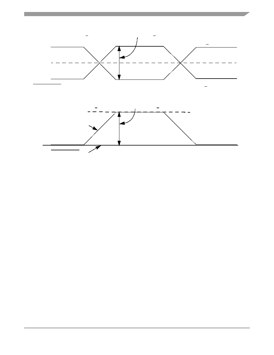
Figure 60. Differential Reference Clock Input DC Requirements (External AC-Coupled)
Figure 61. Single-Ended Reference Clock Input DC Requirements
2.20.2.3
Interfacing With Other Differential Signaling Levels
With on-chip termination to SnGND (xcorevss), the differential reference clocks inputs are HCSL (High-Speed Current
Steering Logic) compatible DC-coupled.
Many other low voltage differential type outputs like LVDS (Low Voltage Differential Signaling) can be used but may need to
be AC-coupled due to the limited common mode input range allowed (100 to 400 mV) for DC-coupled connection.
LVPECL (Low Voltage Positive Emitter-Coupled Logic) outputs can produce signal with too large amplitude and may need to
be DC-biased at clock driver output first, then followed with series attenuation resistor to reduce the amplitude, in addition to
AC-coupling.
NOTE
driver chip's internal structure, output impedance and termination requirements are
different between various clock driver chip manufacturers, it is very possible that the clock
circuit reference designs provided by clock driver chip vendor are different from what is
shown below. They might also vary from one vendor to the other. Therefore, Freescale
Semiconductor can neither provide the optimal clock driver reference circuits, nor
guarantee the correctness of the following clock driver connection reference circuits. The
system designer is recommended to contact the selected clock driver chip vendor for the
optimal reference circuits with the chip’s SerDes reference clock receiver requirement
provided in this document.
SD
n_REF_CLK
SD
n_REF_CLK
Vcm
200mV < Input Amplitude or Differential Peak < 800 mV
Vmax < Vcm + 400 mV
Vmin > Vcm – 400 mV
SD
n_REF_CLK
SD
n_REF_CLK
400 mV < SD
n_REF_CLK Input Amplitude < 800 mV
0V
相关PDF资料 |
PDF描述 |
|---|---|
| GSC60DTES | CONN EDGECARD 120POS .100 EYELET |
| MPC8536EBVTAULA | MPU PWRQUICC III 1333MHZ 783PBGA |
| AMM36DTMI | CONN EDGECARD 72POS R/A .156 SLD |
| 2-1734248-6 | CONN FPC/ZIP 26POS 1MM VERT SMD |
| AMM36DTAI | CONN EDGECARD 72POS R/A .156 SLD |
相关代理商/技术参数 |
参数描述 |
|---|---|
| MPC8536-RDK | 功能描述:开发板和工具包 - 其他处理器 COMEXPRESS BASED MPC8536 RoHS:否 制造商:Freescale Semiconductor 产品:Development Systems 工具用于评估:P3041 核心:e500mc 接口类型:I2C, SPI, USB 工作电源电压: |
| MPC853TVR100A | 功能描述:微处理器 - MPU POWER QUICC I HIP6W RoHS:否 制造商:Atmel 处理器系列:SAMA5D31 核心:ARM Cortex A5 数据总线宽度:32 bit 最大时钟频率:536 MHz 程序存储器大小:32 KB 数据 RAM 大小:128 KB 接口类型:CAN, Ethernet, LIN, SPI,TWI, UART, USB 工作电源电压:1.8 V to 3.3 V 最大工作温度:+ 85 C 安装风格:SMD/SMT 封装 / 箱体:FBGA-324 |
| MPC853TVR66A | 功能描述:微处理器 - MPU POWER QUICC I HIP6W RoHS:否 制造商:Atmel 处理器系列:SAMA5D31 核心:ARM Cortex A5 数据总线宽度:32 bit 最大时钟频率:536 MHz 程序存储器大小:32 KB 数据 RAM 大小:128 KB 接口类型:CAN, Ethernet, LIN, SPI,TWI, UART, USB 工作电源电压:1.8 V to 3.3 V 最大工作温度:+ 85 C 安装风格:SMD/SMT 封装 / 箱体:FBGA-324 |
| MPC853TZT100A | 功能描述:微处理器 - MPU POWER QUICC I HIP6W RoHS:否 制造商:Atmel 处理器系列:SAMA5D31 核心:ARM Cortex A5 数据总线宽度:32 bit 最大时钟频率:536 MHz 程序存储器大小:32 KB 数据 RAM 大小:128 KB 接口类型:CAN, Ethernet, LIN, SPI,TWI, UART, USB 工作电源电压:1.8 V to 3.3 V 最大工作温度:+ 85 C 安装风格:SMD/SMT 封装 / 箱体:FBGA-324 |
| MPC853TZT66A | 功能描述:微处理器 - MPU POWER QUICC I HIP6W RoHS:否 制造商:Atmel 处理器系列:SAMA5D31 核心:ARM Cortex A5 数据总线宽度:32 bit 最大时钟频率:536 MHz 程序存储器大小:32 KB 数据 RAM 大小:128 KB 接口类型:CAN, Ethernet, LIN, SPI,TWI, UART, USB 工作电源电压:1.8 V to 3.3 V 最大工作温度:+ 85 C 安装风格:SMD/SMT 封装 / 箱体:FBGA-324 |
发布紧急采购,3分钟左右您将得到回复。