- 您现在的位置:买卖IC网 > PDF目录3962 > MPC8545EVUATG (Freescale Semiconductor)IC MPU PWRQUICC III 783-FCCBGA PDF资料下载
参数资料
| 型号: | MPC8545EVUATG |
| 厂商: | Freescale Semiconductor |
| 文件页数: | 24/151页 |
| 文件大小: | 0K |
| 描述: | IC MPU PWRQUICC III 783-FCCBGA |
| 标准包装: | 1 |
| 系列: | MPC85xx |
| 处理器类型: | 32-位 MPC85xx PowerQUICC III |
| 速度: | 1.2GHz |
| 电压: | 1.1V |
| 安装类型: | 表面贴装 |
| 封装/外壳: | 783-BBGA,FCBGA |
| 供应商设备封装: | 783-FCPBGA(29x29) |
| 包装: | 托盘 |
第1页第2页第3页第4页第5页第6页第7页第8页第9页第10页第11页第12页第13页第14页第15页第16页第17页第18页第19页第20页第21页第22页第23页当前第24页第25页第26页第27页第28页第29页第30页第31页第32页第33页第34页第35页第36页第37页第38页第39页第40页第41页第42页第43页第44页第45页第46页第47页第48页第49页第50页第51页第52页第53页第54页第55页第56页第57页第58页第59页第60页第61页第62页第63页第64页第65页第66页第67页第68页第69页第70页第71页第72页第73页第74页第75页第76页第77页第78页第79页第80页第81页第82页第83页第84页第85页第86页第87页第88页第89页第90页第91页第92页第93页第94页第95页第96页第97页第98页第99页第100页第101页第102页第103页第104页第105页第106页第107页第108页第109页第110页第111页第112页第113页第114页第115页第116页第117页第118页第119页第120页第121页第122页第123页第124页第125页第126页第127页第128页第129页第130页第131页第132页第133页第134页第135页第136页第137页第138页第139页第140页第141页第142页第143页第144页第145页第146页第147页第148页第149页第150页第151页
MPC8548E PowerQUICC III Integrated Processor Hardware Specifications, Rev. 9
12
Freescale Semiconductor
Electrical Characteristics
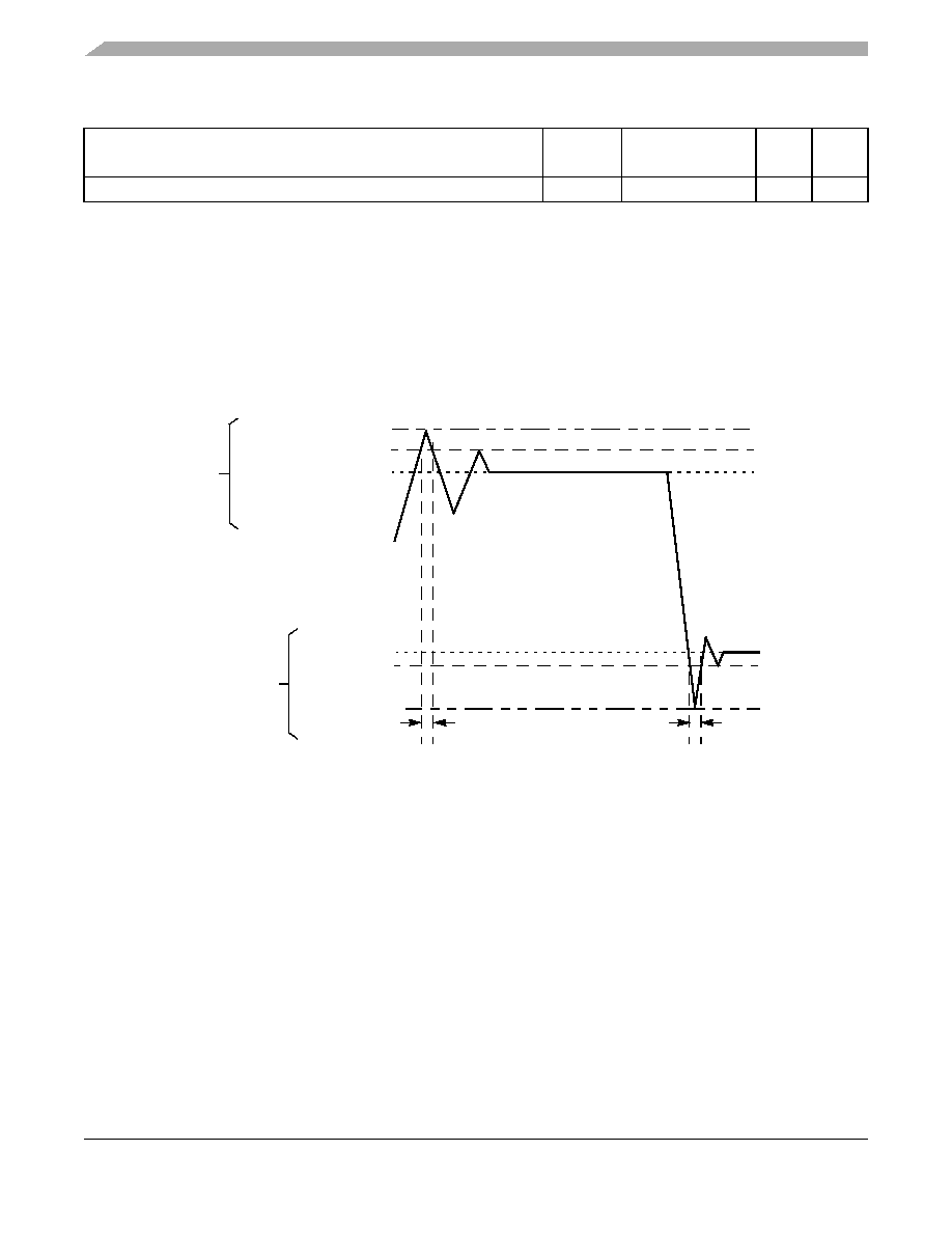
The following figure shows the undershoot and overshoot voltages at the interfaces of this device.
Figure 2. Overshoot/Undershoot Voltage for GVDD/OVDD/LVDD/BVDD/TVDD
The core voltage must always be provided at nominal 1.1 V. Voltage to the processor interface I/Os are
provided through separate sets of supply pins and must be provided at the voltages shown in Table 2. The
input voltage threshold scales with respect to the associated I/O supply voltage. OVDD and LVDD based
receivers are simple CMOS I/O circuits and satisfy appropriate LVCMOS type specifications. The DDR
SDRAM interface uses a single-ended differential receiver referenced the externally supplied MVREF
signal (nominally set to GVDD/2) as is appropriate for the SSTL2 electrical signaling standard.
Junction temperature range
Tj
0 to 105
C—
Notes:
1. This voltage is the input to the filter discussed in Section 22.2, “PLL Power Supply Filtering,” and not necessarily the voltage
at the AVDD pin, which may be reduced from VDD by the filter.
2. Caution: MVIN must not exceed GVDD by more than 0.3 V. This limit may be exceeded for a maximum of 20 ms during
power-on reset and power-down sequences.
3. Caution: OVIN must not exceed OVDD by more than 0.3 V. This limit may be exceeded for a maximum of 20 ms during
power-on reset and power-down sequences.
4. Caution: L/TVIN must not exceed L/TVDD by more than 0.3 V. This limit may be exceeded for a maximum of 20 ms during
power-on reset and power-down sequences.
Table 2. Recommended Operating Conditions (continued)
Characteristic
Symbol
Recommended
Value
Unit
Notes
GND
GND – 0.3 V
GND – 0.7 V
Not to Exceed 10%
B/G/L/O/TVDD + 20%
B/G/L/O/TVDD
B/G/L/O/TVDD + 5%
of tCLOCK
1
1. tCLOCK refers to the clock period associated with the respective interface:
VIH
VIL
Notes:
2. Note that with the PCI overshoot allowed (as specified above), the device
does not fully comply with the maximum AC ratings and device protection
guideline outlined in the PCI rev. 2.2 standard (section 4.2.2.3).
For I2C and JTAG, tCLOCK references SYSCLK.
For DDR, tCLOCK references MCLK.
For eTSEC, tCLOCK references EC_GTX_CLK125.
For LBIU, tCLOCK references LCLK.
For PCI, tCLOCK references PCIn_CLK or SYSCLK.
For SerDes, tCLOCK references SD_REF_CLK.
相关PDF资料 |
PDF描述 |
|---|---|
| IDT70V3319S166PRF8 | IC SRAM 4MBIT 166MHZ 128TQFP |
| IDT70T659S10BFI8 | IC SRAM 4MBIT 10NS 208FBGA |
| MPC8547EHXAUJ | IC MPU PWRQUICC III 783-FCCBGA |
| IDT70T659S10BCI8 | IC SRAM 4MBIT 10NS 256BGA |
| IDT70T631S10BFI8 | IC SRAM 4MBIT 10NS 208FBGA |
相关代理商/技术参数 |
参数描述 |
|---|---|
| MPC8545HXANG | 功能描述:微处理器 - MPU PQ38 8548 RoHS:否 制造商:Atmel 处理器系列:SAMA5D31 核心:ARM Cortex A5 数据总线宽度:32 bit 最大时钟频率:536 MHz 程序存储器大小:32 KB 数据 RAM 大小:128 KB 接口类型:CAN, Ethernet, LIN, SPI,TWI, UART, USB 工作电源电压:1.8 V to 3.3 V 最大工作温度:+ 85 C 安装风格:SMD/SMT 封装 / 箱体:FBGA-324 |
| MPC8545HXAQG | 功能描述:微处理器 - MPU PQ38 8548 RoHS:否 制造商:Atmel 处理器系列:SAMA5D31 核心:ARM Cortex A5 数据总线宽度:32 bit 最大时钟频率:536 MHz 程序存储器大小:32 KB 数据 RAM 大小:128 KB 接口类型:CAN, Ethernet, LIN, SPI,TWI, UART, USB 工作电源电压:1.8 V to 3.3 V 最大工作温度:+ 85 C 安装风格:SMD/SMT 封装 / 箱体:FBGA-324 |
| MPC8545HXATG | 功能描述:微处理器 - MPU PQ38 8548 RoHS:否 制造商:Atmel 处理器系列:SAMA5D31 核心:ARM Cortex A5 数据总线宽度:32 bit 最大时钟频率:536 MHz 程序存储器大小:32 KB 数据 RAM 大小:128 KB 接口类型:CAN, Ethernet, LIN, SPI,TWI, UART, USB 工作电源电压:1.8 V to 3.3 V 最大工作温度:+ 85 C 安装风格:SMD/SMT 封装 / 箱体:FBGA-324 |
| MPC8545PXANGA | 功能描述:微处理器 - MPU PQ3 8545 RoHS:否 制造商:Atmel 处理器系列:SAMA5D31 核心:ARM Cortex A5 数据总线宽度:32 bit 最大时钟频率:536 MHz 程序存储器大小:32 KB 数据 RAM 大小:128 KB 接口类型:CAN, Ethernet, LIN, SPI,TWI, UART, USB 工作电源电压:1.8 V to 3.3 V 最大工作温度:+ 85 C 安装风格:SMD/SMT 封装 / 箱体:FBGA-324 |
| MPC8545PXANGB | 功能描述:微处理器 - MPU FG PQ38 8548 RoHS:否 制造商:Atmel 处理器系列:SAMA5D31 核心:ARM Cortex A5 数据总线宽度:32 bit 最大时钟频率:536 MHz 程序存储器大小:32 KB 数据 RAM 大小:128 KB 接口类型:CAN, Ethernet, LIN, SPI,TWI, UART, USB 工作电源电压:1.8 V to 3.3 V 最大工作温度:+ 85 C 安装风格:SMD/SMT 封装 / 箱体:FBGA-324 |
发布紧急采购,3分钟左右您将得到回复。