- 您现在的位置:买卖IC网 > PDF目录69036 > MPC8560PXALDB (FREESCALE SEMICONDUCTOR INC) 32-BIT, 667 MHz, RISC PROCESSOR, PBGA783 PDF资料下载
参数资料
| 型号: | MPC8560PXALDB |
| 厂商: | FREESCALE SEMICONDUCTOR INC |
| 元件分类: | 微控制器/微处理器 |
| 英文描述: | 32-BIT, 667 MHz, RISC PROCESSOR, PBGA783 |
| 封装: | 29 X 29 MM, 3.75 MM HEIGHT, 1 MM PITCH, FLIP CHIP, PLASTIC, BGA-783 |
| 文件页数: | 62/108页 |
| 文件大小: | 2170K |
| 代理商: | MPC8560PXALDB |
第1页第2页第3页第4页第5页第6页第7页第8页第9页第10页第11页第12页第13页第14页第15页第16页第17页第18页第19页第20页第21页第22页第23页第24页第25页第26页第27页第28页第29页第30页第31页第32页第33页第34页第35页第36页第37页第38页第39页第40页第41页第42页第43页第44页第45页第46页第47页第48页第49页第50页第51页第52页第53页第54页第55页第56页第57页第58页第59页第60页第61页当前第62页第63页第64页第65页第66页第67页第68页第69页第70页第71页第72页第73页第74页第75页第76页第77页第78页第79页第80页第81页第82页第83页第84页第85页第86页第87页第88页第89页第90页第91页第92页第93页第94页第95页第96页第97页第98页第99页第100页第101页第102页第103页第104页第105页第106页第107页第108页
MPC8560 Integrated Processor Hardware Specifications, Rev. 3.1
Freescale Semiconductor
57
PCI/PCI-X
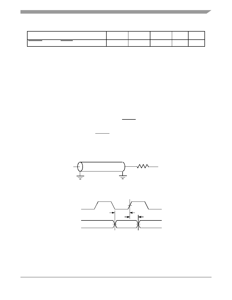
Figure 38 provides the AC test load for PCI and PCI-X.
Figure 38. PCI/PCI-X AC Test Load
Figure 39 shows the PCI/PCI-X input AC timing conditions.
Figure 39. PCI-PCI-X Input AC Timing Measurement Conditions
HRESET high to first FRAME assertion
tPCRHFV
10
—
clocks
8, 11
Notes:
1.Note that the symbols used for timing specifications herein follow the pattern of t(first two letters of functional
block)(signal)(state) (reference)(state) for inputs and t(first two letters of functional block)(reference)(state)(signal)(state) for outputs. For
example, tPCIVKH symbolizes PCI/PCI-X timing (PC) with respect to the time the input signals (I) reach the valid
state (V) relative to the SYSCLK clock, tSYS, reference (K) going to the high (H) state or setup time. Also, tPCRHFV
symbolizes PCI/PCI-X timing (PC) with respect to the time hard reset (R) went high (H) relative to the frame signal
(F) going to the valid (V) state.
2.See the timing measurement conditions in the PCI 2.2 Local Bus Specifications.
3.All PCI signals are measured from OVDD/2 of the rising edge of PCI_SYNC_IN to 0.4 × OVDD of the signal in
question for 3.3 V PCI signaling levels.
4.For purposes of active/float timing measurements, the Hi-Z or off state is defined to be when the total current
delivered through the component pin is less than or equal to the leakage current specification.
5.Input timings are measured at the pin.
6.The timing parameter tSYS indicates the minimum and maximum CLK cycle times for the various specified
frequencies. The system clock period must be kept within the minimum and maximum defined ranges. For values
7.The setup and hold time is with respect to the rising edge of HRESET.
8.The timing parameter tPCRHFV is a minimum of 10 clocks rather than the minimum of 5 clocks in the PCI 2.2 Local
Bus Specifications.
9.The reset assertion timing requirement for HRESET is 100
s.
10.Guaranteed by characterization.
11.Guaranteed by design.
Table 42. PCI AC Timing Specifications at 66 MHz (continued)
Parameter
Symbol 1
Min
Max
Unit
Notes
Output
OVDD/2
RL = 50
Z0 = 50
tPCIVKH
CLK
Input
tPCIXKH
相关PDF资料 |
PDF描述 |
|---|---|
| MPC8560CPXALFB | 32-BIT, 667 MHz, RISC PROCESSOR, PBGA783 |
| MPC866PCZP100 | 32-BIT, 100 MHz, RISC PROCESSOR, PBGA256 |
| MPC866TCZP100 | 32-BIT, 100 MHz, RISC PROCESSOR, PBGA256 |
| MPC866TZP133A | 32-BIT, 133 MHz, RISC PROCESSOR, PBGA357 |
| MPC866PZP133A | 32-BIT, 133 MHz, RISC PROCESSOR, PBGA357 |
相关代理商/技术参数 |
参数描述 |
|---|---|
| MPC8560PXAQFB | 功能描述:微处理器 - MPU PQ 3 DRACO-DRACOM RoHS:否 制造商:Atmel 处理器系列:SAMA5D31 核心:ARM Cortex A5 数据总线宽度:32 bit 最大时钟频率:536 MHz 程序存储器大小:32 KB 数据 RAM 大小:128 KB 接口类型:CAN, Ethernet, LIN, SPI,TWI, UART, USB 工作电源电压:1.8 V to 3.3 V 最大工作温度:+ 85 C 安装风格:SMD/SMT 封装 / 箱体:FBGA-324 |
| MPC8560PXAQFC | 功能描述:微处理器 - MPU PQ 3 DRACO-DRACOM RoHS:否 制造商:Atmel 处理器系列:SAMA5D31 核心:ARM Cortex A5 数据总线宽度:32 bit 最大时钟频率:536 MHz 程序存储器大小:32 KB 数据 RAM 大小:128 KB 接口类型:CAN, Ethernet, LIN, SPI,TWI, UART, USB 工作电源电压:1.8 V to 3.3 V 最大工作温度:+ 85 C 安装风格:SMD/SMT 封装 / 箱体:FBGA-324 |
| MPC8560VT667LB | 功能描述:微处理器 - MPU PQ 3 8560-DRACOM RoHS:否 制造商:Atmel 处理器系列:SAMA5D31 核心:ARM Cortex A5 数据总线宽度:32 bit 最大时钟频率:536 MHz 程序存储器大小:32 KB 数据 RAM 大小:128 KB 接口类型:CAN, Ethernet, LIN, SPI,TWI, UART, USB 工作电源电压:1.8 V to 3.3 V 最大工作温度:+ 85 C 安装风格:SMD/SMT 封装 / 箱体:FBGA-324 |
| MPC8560VT667LC | 功能描述:微处理器 - MPU PQ 3 8560-DRACOM RoHS:否 制造商:Atmel 处理器系列:SAMA5D31 核心:ARM Cortex A5 数据总线宽度:32 bit 最大时钟频率:536 MHz 程序存储器大小:32 KB 数据 RAM 大小:128 KB 接口类型:CAN, Ethernet, LIN, SPI,TWI, UART, USB 工作电源电压:1.8 V to 3.3 V 最大工作温度:+ 85 C 安装风格:SMD/SMT 封装 / 箱体:FBGA-324 |
| MPC8560VT833LB | 功能描述:微处理器 - MPU PQ 3 8560-DRACOM RoHS:否 制造商:Atmel 处理器系列:SAMA5D31 核心:ARM Cortex A5 数据总线宽度:32 bit 最大时钟频率:536 MHz 程序存储器大小:32 KB 数据 RAM 大小:128 KB 接口类型:CAN, Ethernet, LIN, SPI,TWI, UART, USB 工作电源电压:1.8 V to 3.3 V 最大工作温度:+ 85 C 安装风格:SMD/SMT 封装 / 箱体:FBGA-324 |
发布紧急采购,3分钟左右您将得到回复。