- 您现在的位置:买卖IC网 > PDF目录69036 > MPC8560PXALDB (FREESCALE SEMICONDUCTOR INC) 32-BIT, 667 MHz, RISC PROCESSOR, PBGA783 PDF资料下载
参数资料
| 型号: | MPC8560PXALDB |
| 厂商: | FREESCALE SEMICONDUCTOR INC |
| 元件分类: | 微控制器/微处理器 |
| 英文描述: | 32-BIT, 667 MHz, RISC PROCESSOR, PBGA783 |
| 封装: | 29 X 29 MM, 3.75 MM HEIGHT, 1 MM PITCH, FLIP CHIP, PLASTIC, BGA-783 |
| 文件页数: | 69/108页 |
| 文件大小: | 2170K |
| 代理商: | MPC8560PXALDB |
第1页第2页第3页第4页第5页第6页第7页第8页第9页第10页第11页第12页第13页第14页第15页第16页第17页第18页第19页第20页第21页第22页第23页第24页第25页第26页第27页第28页第29页第30页第31页第32页第33页第34页第35页第36页第37页第38页第39页第40页第41页第42页第43页第44页第45页第46页第47页第48页第49页第50页第51页第52页第53页第54页第55页第56页第57页第58页第59页第60页第61页第62页第63页第64页第65页第66页第67页第68页当前第69页第70页第71页第72页第73页第74页第75页第76页第77页第78页第79页第80页第81页第82页第83页第84页第85页第86页第87页第88页第89页第90页第91页第92页第93页第94页第95页第96页第97页第98页第99页第100页第101页第102页第103页第104页第105页第106页第107页第108页
MPC8560 Integrated Processor Hardware Specifications, Rev. 3.1
Freescale Semiconductor
63
RapidIO
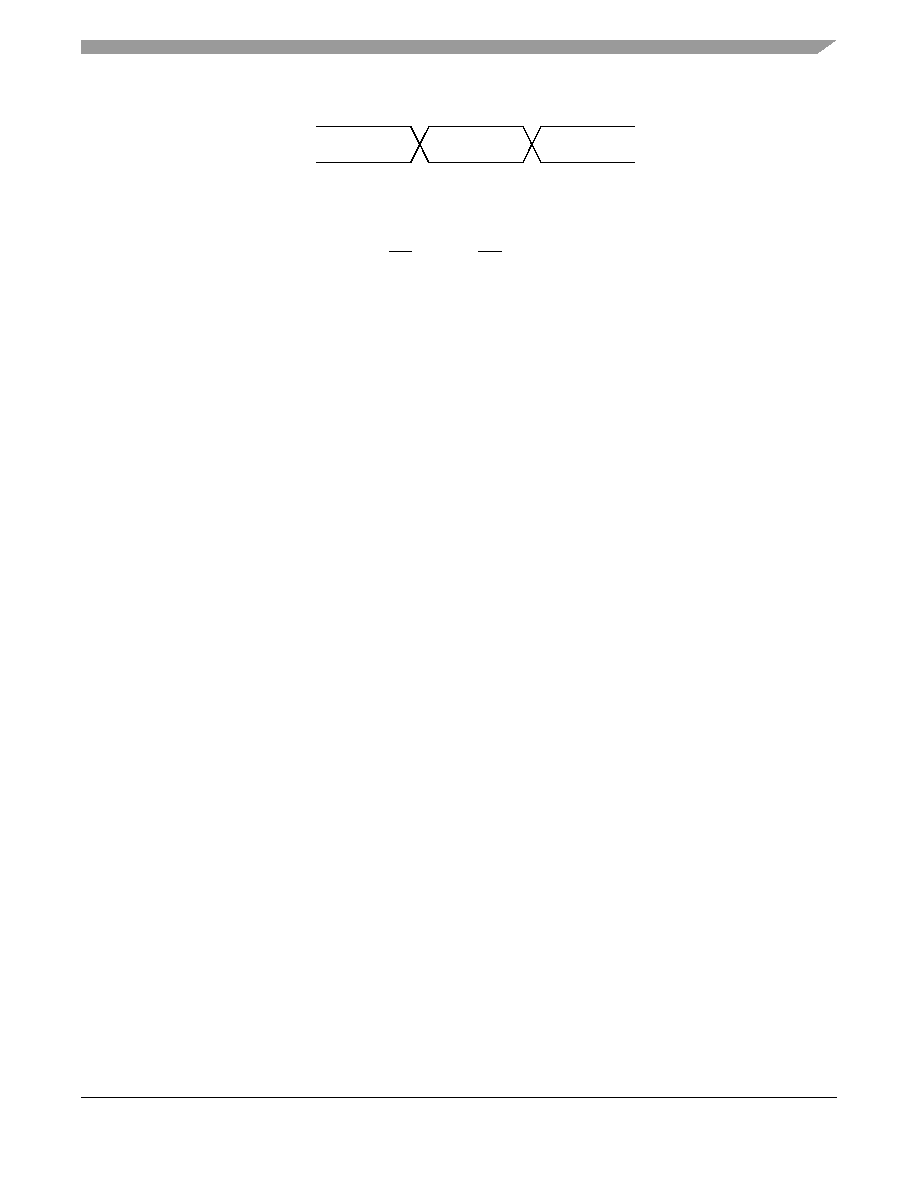
Figure 42. Differential Peak-to-Peak Voltage of Transmitter or Receiver
To illustrate these definitions using numerical values, consider the case where a LVDS transmitter has a common
mode voltage of 1.2 V and each signal has a swing that goes between 1.4 and 1.0 V. Using these values, the
peak-to-peak voltage swing of the signals TD, TD, RD, and RD is 400 mV. The differential signal ranges between
400 and –400 mV. The peak differential signal is 400 mV, and the peak-to-peak differential signal is 800 mV.
A timing edge is the zero-crossing of a differential signal. Each skew timing parameter on a parallel bus is
synchronously measured on two signals relative to each other in the same cycle, such as data to data, data to clock,
or clock to clock. A skew timing parameter may be relative to the edge of a signal or to the middle of two sequential
edges.
Static skew represents the timing difference between signals that does not vary over time regardless of system
activity or data pattern. Path length differences are a primary source of static skew.
Dynamic skew represents the amount of timing difference between signals that is dependent on the activity of other
signals and varies over time. Crosstalk between signals is a source of dynamic skew.
Eye diagrams and compliance masks are a useful way to visualize and specify driver and receiver performance. This
technique is used in several serial bus specifications. An example compliance mask is shown in Figure 43. The key
difference in the application of this technique for a parallel bus is that the data is source synchronous to its bus clock
while serial data is referenced to its embedded clock. Eye diagrams reveal the quality (cleanness, openness,
goodness) of a driver output or receiver input. An advantage of using an eye diagram and a compliance mask is that
it allows specifying the quality of a signal without requiring separate specifications for effects such as rise time, duty
cycle distortion, data dependent dynamic skew, random dynamic skew, etc. This allows the individual
semiconductor manufacturer maximum flexibility to trade off various performance criteria while keeping the system
performance constant.
In using the eye pattern and compliance mask approach, the quality of the signal is specified by the compliance
mask. The mask specifies the maximum permissible magnitude of the signal and the minimum permissible eye
opening. The eye diagram for the signal under test is generated according to the specification. Compliance is
determined by whether the compliance mask can be positioned over the eye diagram such that the eye pattern falls
entirely within the unshaded portion of the mask.
Serial specifications have clock encoded with the data, but the LP-LVDS physical layer defined by RapidIO is a
source synchronous parallel port so additional specifications to include effects that are not found in serial links are
required. Specifications for the effect of bit to bit timing differences caused by static skew have been added and the
eye diagrams specified are measured relative to the associated clock in order to include clock to data effects. With
the transmit output (or receiver input) eye diagram, the user can determine if the transmitter output (or receiver
input) is compliant with an oscilloscope with the appropriate software.
A V
B V
TD or RD
相关PDF资料 |
PDF描述 |
|---|---|
| MPC8560CPXALFB | 32-BIT, 667 MHz, RISC PROCESSOR, PBGA783 |
| MPC866PCZP100 | 32-BIT, 100 MHz, RISC PROCESSOR, PBGA256 |
| MPC866TCZP100 | 32-BIT, 100 MHz, RISC PROCESSOR, PBGA256 |
| MPC866TZP133A | 32-BIT, 133 MHz, RISC PROCESSOR, PBGA357 |
| MPC866PZP133A | 32-BIT, 133 MHz, RISC PROCESSOR, PBGA357 |
相关代理商/技术参数 |
参数描述 |
|---|---|
| MPC8560PXAQFB | 功能描述:微处理器 - MPU PQ 3 DRACO-DRACOM RoHS:否 制造商:Atmel 处理器系列:SAMA5D31 核心:ARM Cortex A5 数据总线宽度:32 bit 最大时钟频率:536 MHz 程序存储器大小:32 KB 数据 RAM 大小:128 KB 接口类型:CAN, Ethernet, LIN, SPI,TWI, UART, USB 工作电源电压:1.8 V to 3.3 V 最大工作温度:+ 85 C 安装风格:SMD/SMT 封装 / 箱体:FBGA-324 |
| MPC8560PXAQFC | 功能描述:微处理器 - MPU PQ 3 DRACO-DRACOM RoHS:否 制造商:Atmel 处理器系列:SAMA5D31 核心:ARM Cortex A5 数据总线宽度:32 bit 最大时钟频率:536 MHz 程序存储器大小:32 KB 数据 RAM 大小:128 KB 接口类型:CAN, Ethernet, LIN, SPI,TWI, UART, USB 工作电源电压:1.8 V to 3.3 V 最大工作温度:+ 85 C 安装风格:SMD/SMT 封装 / 箱体:FBGA-324 |
| MPC8560VT667LB | 功能描述:微处理器 - MPU PQ 3 8560-DRACOM RoHS:否 制造商:Atmel 处理器系列:SAMA5D31 核心:ARM Cortex A5 数据总线宽度:32 bit 最大时钟频率:536 MHz 程序存储器大小:32 KB 数据 RAM 大小:128 KB 接口类型:CAN, Ethernet, LIN, SPI,TWI, UART, USB 工作电源电压:1.8 V to 3.3 V 最大工作温度:+ 85 C 安装风格:SMD/SMT 封装 / 箱体:FBGA-324 |
| MPC8560VT667LC | 功能描述:微处理器 - MPU PQ 3 8560-DRACOM RoHS:否 制造商:Atmel 处理器系列:SAMA5D31 核心:ARM Cortex A5 数据总线宽度:32 bit 最大时钟频率:536 MHz 程序存储器大小:32 KB 数据 RAM 大小:128 KB 接口类型:CAN, Ethernet, LIN, SPI,TWI, UART, USB 工作电源电压:1.8 V to 3.3 V 最大工作温度:+ 85 C 安装风格:SMD/SMT 封装 / 箱体:FBGA-324 |
| MPC8560VT833LB | 功能描述:微处理器 - MPU PQ 3 8560-DRACOM RoHS:否 制造商:Atmel 处理器系列:SAMA5D31 核心:ARM Cortex A5 数据总线宽度:32 bit 最大时钟频率:536 MHz 程序存储器大小:32 KB 数据 RAM 大小:128 KB 接口类型:CAN, Ethernet, LIN, SPI,TWI, UART, USB 工作电源电压:1.8 V to 3.3 V 最大工作温度:+ 85 C 安装风格:SMD/SMT 封装 / 箱体:FBGA-324 |
发布紧急采购,3分钟左右您将得到回复。