- 您现在的位置:买卖IC网 > PDF目录4035 > MPC8572ECVTAVNE (Freescale Semiconductor)MPU POWERQUICC III 1023FCPBGA PDF资料下载
参数资料
| 型号: | MPC8572ECVTAVNE |
| 厂商: | Freescale Semiconductor |
| 文件页数: | 53/138页 |
| 文件大小: | 0K |
| 描述: | MPU POWERQUICC III 1023FCPBGA |
| 标准包装: | 1 |
| 系列: | MPC85xx |
| 处理器类型: | 32-位 MPC85xx PowerQUICC III |
| 速度: | 1.5GHz |
| 电压: | 1.1V |
| 安装类型: | 表面贴装 |
| 封装/外壳: | 1023-BBGA,FCBGA |
| 供应商设备封装: | 1023-FCPBGA(33x33) |
| 包装: | 托盘 |
第1页第2页第3页第4页第5页第6页第7页第8页第9页第10页第11页第12页第13页第14页第15页第16页第17页第18页第19页第20页第21页第22页第23页第24页第25页第26页第27页第28页第29页第30页第31页第32页第33页第34页第35页第36页第37页第38页第39页第40页第41页第42页第43页第44页第45页第46页第47页第48页第49页第50页第51页第52页当前第53页第54页第55页第56页第57页第58页第59页第60页第61页第62页第63页第64页第65页第66页第67页第68页第69页第70页第71页第72页第73页第74页第75页第76页第77页第78页第79页第80页第81页第82页第83页第84页第85页第86页第87页第88页第89页第90页第91页第92页第93页第94页第95页第96页第97页第98页第99页第100页第101页第102页第103页第104页第105页第106页第107页第108页第109页第110页第111页第112页第113页第114页第115页第116页第117页第118页第119页第120页第121页第122页第123页第124页第125页第126页第127页第128页第129页第130页第131页第132页第133页第134页第135页第136页第137页第138页
MPC8572E PowerQUICC III Integrated Processor Hardware Specifications, Rev. 5
Freescale Semiconductor
21
DDR2 and DDR3 SDRAM Controller
this section for DDR3 is applicable for data rate between 606 MHz and 800 MHz, as long as the DC and
AC specifications of the DDR3 memory to be used are compliant to both JEDEC specifications as well as
the specifications and requirements described in this MPC8572E hardware specifications document.
6.2.1
DDR2 and DDR3 SDRAM Interface Input AC Timing Specifications
Table 15, Table 16, and Table 17 provide the input AC timing specifications for the DDR controller when
interfacing to DDR2 and DDR3 SDRAM.
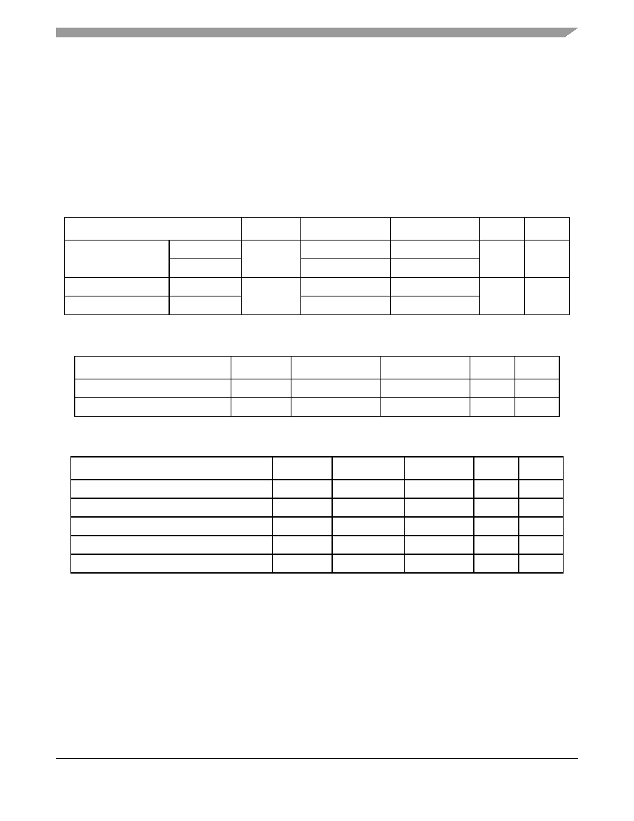
Table 15. DDR2 SDRAM Interface Input AC Timing Specifications for 1.8-V Interface
At recommended operating conditions with GVDD of 1.8 V ± 5%
Parameter
Symbol
Min
Max
Unit
Notes
AC input low voltage
>=667 MHz
VILAC
—MVREFn – 0.20
V
—
<= 533 MHz
—
MVREFn – 0.25
AC input high voltage
>=667 MHz
VIHAC
MVREFn + 0.20
—
V
—
<= 533 MHz
MVREFn + 0.25
—
Table 16. DDR3 SDRAM Interface Input AC Timing Specifications for 1.5-V Interface
At recommended operating conditions with GVDD of 1.5 V ± 5%. DDR3 data rate is between 606 MHz and 800 MHz.
Parameter
Symbol
Min
Max
Unit
Notes
AC input low voltage
VILAC
—MVREFn – 0.175
V
—
AC input high voltage
VIHAC
MVREFn + 0.175
—
V
—
Table 17. DDR2 and DDR3 SDRAM Interface Input AC Timing Specifications
At recommended operating conditions with GVDD of 1.8 V ± 5% for DDR2 or 1.5 V ± 5% for DDR3.
Parameter
Symbol
Min
Max
Unit
Notes
Controller Skew for MDQS—MDQ/MECC
tCISKEW
—
ps
1, 2
800 MHz
—
–200
200
—
667 MHz
—
–240
240
—
533 MHz
—
–300
300
—
400 MHz
—
–365
365
—
Note:
1. tCISKEW represents the total amount of skew consumed by the controller between MDQS[n] and any corresponding
bit that is captured with MDQS[n]. This should be subtracted from the total timing budget.
2. The amount of skew that can be tolerated from MDQS to a corresponding MDQ signal is called tDISKEW.This can be
determined by the following equation: tDISKEW =+/–(T/4 – abs(tCISKEW)) where T is the clock period and
abs(tCISKEW) is the absolute value of tCISKEW.
相关PDF资料 |
PDF描述 |
|---|---|
| MC68EN360RC25L | IC MPU QUICC 32BIT 25MHZ 241-PGA |
| ABB106DHAN-S621 | CONN EDGECARD 212PS R/A .050 SLD |
| MPC8265AZUPJDC | IC MPU POWERQUICC II 480-TBGA |
| MC68EC040FE40A | IC MPU 32BIT 40MHZ 184-CQFP |
| MPC8545EVTANGB | MPU POWERQUICC III 783-PBGA |
相关代理商/技术参数 |
参数描述 |
|---|---|
| MPC8572ELPXARLD | 功能描述:微处理器 - MPU 32-BIT CMOS 1.067GHz RoHS:否 制造商:Atmel 处理器系列:SAMA5D31 核心:ARM Cortex A5 数据总线宽度:32 bit 最大时钟频率:536 MHz 程序存储器大小:32 KB 数据 RAM 大小:128 KB 接口类型:CAN, Ethernet, LIN, SPI,TWI, UART, USB 工作电源电压:1.8 V to 3.3 V 最大工作温度:+ 85 C 安装风格:SMD/SMT 封装 / 箱体:FBGA-324 |
| MPC8572ELPXARLE | 功能描述:微处理器 - MPU 38H R211 Enc SnPb 1067LP RoHS:否 制造商:Atmel 处理器系列:SAMA5D31 核心:ARM Cortex A5 数据总线宽度:32 bit 最大时钟频率:536 MHz 程序存储器大小:32 KB 数据 RAM 大小:128 KB 接口类型:CAN, Ethernet, LIN, SPI,TWI, UART, USB 工作电源电压:1.8 V to 3.3 V 最大工作温度:+ 85 C 安装风格:SMD/SMT 封装 / 箱体:FBGA-324 |
| MPC8572ELPXATLD | 功能描述:微处理器 - MPU 32-BIT CMOS 1.2GHz RoHS:否 制造商:Atmel 处理器系列:SAMA5D31 核心:ARM Cortex A5 数据总线宽度:32 bit 最大时钟频率:536 MHz 程序存储器大小:32 KB 数据 RAM 大小:128 KB 接口类型:CAN, Ethernet, LIN, SPI,TWI, UART, USB 工作电源电压:1.8 V to 3.3 V 最大工作温度:+ 85 C 安装风格:SMD/SMT 封装 / 箱体:FBGA-324 |
| MPC8572ELPXATLE | 功能描述:微处理器 - MPU 38H R211 Enc SnPb 1200LP RoHS:否 制造商:Atmel 处理器系列:SAMA5D31 核心:ARM Cortex A5 数据总线宽度:32 bit 最大时钟频率:536 MHz 程序存储器大小:32 KB 数据 RAM 大小:128 KB 接口类型:CAN, Ethernet, LIN, SPI,TWI, UART, USB 工作电源电压:1.8 V to 3.3 V 最大工作温度:+ 85 C 安装风格:SMD/SMT 封装 / 箱体:FBGA-324 |
| MPC8572ELPXAULD | 功能描述:微处理器 - MPU 32-BIT CMOS 1.333GHz RoHS:否 制造商:Atmel 处理器系列:SAMA5D31 核心:ARM Cortex A5 数据总线宽度:32 bit 最大时钟频率:536 MHz 程序存储器大小:32 KB 数据 RAM 大小:128 KB 接口类型:CAN, Ethernet, LIN, SPI,TWI, UART, USB 工作电源电压:1.8 V to 3.3 V 最大工作温度:+ 85 C 安装风格:SMD/SMT 封装 / 箱体:FBGA-324 |
发布紧急采购,3分钟左右您将得到回复。