- 您现在的位置:买卖IC网 > PDF目录4041 > MPC8572EVTARLE (Freescale Semiconductor)MPU POWERQUICC III 1023FCPBGA PDF资料下载
参数资料
| 型号: | MPC8572EVTARLE |
| 厂商: | Freescale Semiconductor |
| 文件页数: | 47/138页 |
| 文件大小: | 0K |
| 描述: | MPU POWERQUICC III 1023FCPBGA |
| 标准包装: | 1 |
| 系列: | MPC85xx |
| 处理器类型: | 32-位 MPC85xx PowerQUICC III |
| 速度: | 1.067GHz |
| 电压: | 1.1V |
| 安装类型: | 表面贴装 |
| 封装/外壳: | 1023-BBGA,FCBGA |
| 供应商设备封装: | 1023-FCPBGA(33x33) |
| 包装: | 托盘 |
第1页第2页第3页第4页第5页第6页第7页第8页第9页第10页第11页第12页第13页第14页第15页第16页第17页第18页第19页第20页第21页第22页第23页第24页第25页第26页第27页第28页第29页第30页第31页第32页第33页第34页第35页第36页第37页第38页第39页第40页第41页第42页第43页第44页第45页第46页当前第47页第48页第49页第50页第51页第52页第53页第54页第55页第56页第57页第58页第59页第60页第61页第62页第63页第64页第65页第66页第67页第68页第69页第70页第71页第72页第73页第74页第75页第76页第77页第78页第79页第80页第81页第82页第83页第84页第85页第86页第87页第88页第89页第90页第91页第92页第93页第94页第95页第96页第97页第98页第99页第100页第101页第102页第103页第104页第105页第106页第107页第108页第109页第110页第111页第112页第113页第114页第115页第116页第117页第118页第119页第120页第121页第122页第123页第124页第125页第126页第127页第128页第129页第130页第131页第132页第133页第134页第135页第136页第137页第138页
MPC8572E PowerQUICC III Integrated Processor Hardware Specifications, Rev. 5
16
Freescale Semiconductor
Input Clocks
4
Input Clocks
4.1
System Clock Timing
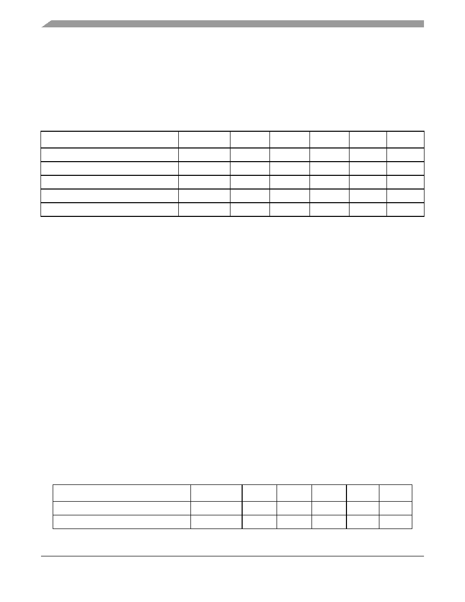
Table 6 provides the system clock (SYSCLK) AC timing specifications for the MPC8572E.
4.2
Real Time Clock Timing
The RTC input is sampled by the platform clock (CCB clock). The output of the sampling latch is then
used as an input to the counters of the PIC and the TimeBase unit of the e500. There is no jitter
specification. The minimum pulse width of the RTC signal should be greater than 2x the period of the CCB
clock. That is, minimum clock high time is 2
× tCCB, and minimum clock low time is 2 × tCCB. There is
no minimum RTC frequency; RTC may be grounded if not needed.
4.3
eTSEC Gigabit Reference Clock Timing
Table 7 provides the eTSEC gigabit reference clocks (EC_GTX_CLK125) AC timing specifications for
the MPC8572E.
Table 6. SYSCLK AC Timing Specifications
At recommended operating conditions with OVDD of 3.3V ± 5%.
Parameter/Condition
Symbol
Min
Typical
Max
Unit
Notes
SYSCLK frequency
fSYSCLK
33
—
133
MHz
1
SYSCLK cycle time
tSYSCLK
7.5
—
30.3
ns
—
SYSCLK rise and fall time
tKH, tKL
0.61.0
1.2ns
2
SYSCLK duty cycle
tKHK/tSYSCLK
40
—
60
%
3
SYSCLK jitter
—
+/– 150
ps
4, 5, 6
Notes:
1. Caution: The CCB clock to SYSCLK ratio and e500 core to CCB clock ratio settings must be chosen such that the resulting
SYSCLK frequency, e500 (core) frequency, and CCB clock frequency do not exceed their respective maximum or minimum
operating frequencies.Refer to Section 19.2, “CCB/SYSCLK PLL Ratio,” and Section 19.3, “e500 Core PLL Ratio,” for ratio
settings.
2. Rise and fall times for SYSCLK are measured at 0.6 V and 2.7 V.
3. Timing is guaranteed by design and characterization.
4. This represents the total input jitter—short term and long term—and is guaranteed by design.
5. The SYSCLK driver’s closed loop jitter bandwidth should be <500 kHz at –20 dB. The bandwidth must be set low to allow
cascade-connected PLL-based devices to track SYSCLK drivers with the specified jitter.
6. For spread spectrum clocking, guidelines are +0% to –1% down spread at a modulation rate between 20 kHz and 60 kHz on
SYSCLK.
Table 7. EC_GTX_CLK125 AC Timing Specifications
At recommended operating conditions with LVDD/TVDD of 3.3V ± 5% or 2.5V ± 5%
Parameter/Condition
Symbol
Min
Typical
Max
Unit
Notes
EC_GTX_CLK125 frequency
fG125
—125
—
MHz
—
EC_GTX_CLK125 cycle time
tG125
—8
—
ns
—
相关PDF资料 |
PDF描述 |
|---|---|
| MPC8572VTATLD | MPU POWERQUICC III 1023-PBGA |
| IDT70V9089S15PF8 | IC SRAM 512KBIT 15NS 100TQFP |
| MPC8572EPXARLD | MPU POWERQUICC III 1023-PBGA |
| XC4036XL-1HQ160I | IC FPGA I-TEMP 3.3V 1SPD 160HQFP |
| XC4036XL-1HQ160C | IC FPGA C-TEMP 3.3V 1SPD 160HQFP |
相关代理商/技术参数 |
参数描述 |
|---|---|
| MPC8572EVTATLB | 功能描述:微处理器 - MPU RV1.1.1 1200 RoHS:否 制造商:Atmel 处理器系列:SAMA5D31 核心:ARM Cortex A5 数据总线宽度:32 bit 最大时钟频率:536 MHz 程序存储器大小:32 KB 数据 RAM 大小:128 KB 接口类型:CAN, Ethernet, LIN, SPI,TWI, UART, USB 工作电源电压:1.8 V to 3.3 V 最大工作温度:+ 85 C 安装风格:SMD/SMT 封装 / 箱体:FBGA-324 |
| MPC8572EVTATLD | 功能描述:微处理器 - MPU PQ3 1200 MHz DDR 667 MHz RoHS:否 制造商:Atmel 处理器系列:SAMA5D31 核心:ARM Cortex A5 数据总线宽度:32 bit 最大时钟频率:536 MHz 程序存储器大小:32 KB 数据 RAM 大小:128 KB 接口类型:CAN, Ethernet, LIN, SPI,TWI, UART, USB 工作电源电压:1.8 V to 3.3 V 最大工作温度:+ 85 C 安装风格:SMD/SMT 封装 / 箱体:FBGA-324 |
| MPC8572EVTATLE | 功能描述:微处理器 - MPU 38H R211 Enc NoPb 1200 RoHS:否 制造商:Atmel 处理器系列:SAMA5D31 核心:ARM Cortex A5 数据总线宽度:32 bit 最大时钟频率:536 MHz 程序存储器大小:32 KB 数据 RAM 大小:128 KB 接口类型:CAN, Ethernet, LIN, SPI,TWI, UART, USB 工作电源电压:1.8 V to 3.3 V 最大工作温度:+ 85 C 安装风格:SMD/SMT 封装 / 箱体:FBGA-324 |
| MPC8572EVTAULB | 功能描述:微处理器 - MPU RV1.1.1 1333 RoHS:否 制造商:Atmel 处理器系列:SAMA5D31 核心:ARM Cortex A5 数据总线宽度:32 bit 最大时钟频率:536 MHz 程序存储器大小:32 KB 数据 RAM 大小:128 KB 接口类型:CAN, Ethernet, LIN, SPI,TWI, UART, USB 工作电源电压:1.8 V to 3.3 V 最大工作温度:+ 85 C 安装风格:SMD/SMT 封装 / 箱体:FBGA-324 |
| MPC8572EVTAULD | 功能描述:微处理器 - MPU 32-BIT CMOS 1.333GHz RoHS:否 制造商:Atmel 处理器系列:SAMA5D31 核心:ARM Cortex A5 数据总线宽度:32 bit 最大时钟频率:536 MHz 程序存储器大小:32 KB 数据 RAM 大小:128 KB 接口类型:CAN, Ethernet, LIN, SPI,TWI, UART, USB 工作电源电压:1.8 V to 3.3 V 最大工作温度:+ 85 C 安装风格:SMD/SMT 封装 / 箱体:FBGA-324 |
发布紧急采购,3分钟左右您将得到回复。