- 您现在的位置:买卖IC网 > PDF目录80465 > MPC92439FAR2 (FREESCALE SEMICONDUCTOR INC) 900 MHz, OTHER CLOCK GENERATOR, PQFP32 PDF资料下载
参数资料
| 型号: | MPC92439FAR2 |
| 厂商: | FREESCALE SEMICONDUCTOR INC |
| 元件分类: | 时钟产生/分配 |
| 英文描述: | 900 MHz, OTHER CLOCK GENERATOR, PQFP32 |
| 封装: | LQFP-32 |
| 文件页数: | 14/16页 |
| 文件大小: | 288K |
| 代理商: | MPC92439FAR2 |
Advanced Clock Drivers Devices
Freescale Semiconductor
7
MPC92439
PROGRAMMING INTERFACE
Programming the MPC92439
Programming the MPC92439 amounts to properly
configuring the internal PLL dividers to produce the desired
synthesized frequency at the output. The output frequency
can be represented by this formula:
fOUT = fXTAL M ÷ N(1)
where fXTAL is the crystal frequency, M is the PLL feedback-
divider and N is the PLL post-divider. The input frequency and
the selection of the feedback divider M is limited by the VCO-
frequency range. fXTAL and M must be configured to match
the VCO frequency range of 400 to 900 MHz in order to
achieve stable PLL operation:
MMIN = fVCO,MIN ÷ (fXTAL) and
(2)
MMAX = fVCO,MAX ÷ (fXTAL)(3)
For instance, the use of a 16 MHz input frequency requires
the configuration of the PLL feedback divider between M = 25
and M = 56. Table 8 shows the usable VCO frequency and M
divider range for other example input frequencies. Assuming
that a 16 MHz input frequency is used, equation (1) reduces
to:
fOUT = 16 M ÷ N(4)
Substituting N for the four available values for N (1, 2, 4, 8)
yields:
Example Calculation for an 16 MHz Input Frequency
For example, if an output frequency of 384 MHz was
desired, the following steps would be taken to identify the
appropriate M and N values. 384 MHz falls within the
frequency range set by an N value of 2, so N[1:0]=00. For N
= 2, FOUT = 8M and M = FOUT
÷8. Therefore, M = 384 ÷ 8 =
48, so M[6:0] = 0110000. Following this procedure a user can
generate any whole frequency between 50 MHz and 900
MHz. The size of the programmable frequency steps will be
equal to:
fSTEP = fXTAL ÷ N(5)
APPLICATIONS INFORMATION
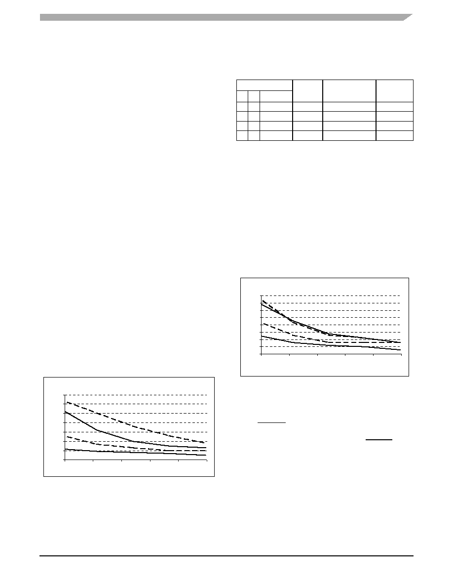
Jitter Performance of the MPC92439
of the MPC92439 across its specified VCO frequency range.
The cycle-to-cycle and period jitter is a function of the VCO
frequency and the output divider N. The general trend is that
as the output frequency increases (higher VCO frequency
and lower N-divider) the MPC92439 output jitter decreases.
Optimum jitter performance can be achieved at higher VCO
and output frequencies. The maximum cycle-to-cycle and
period jitter published in Table 7 correspond to the jitter
performance at the lowest VCO frequency limit).
Figure 4. MPC92439 Cycle-to-cycle Jitter
Figure 5. MPC92439 Period Jitter
Using the Parallel and Serial Interface
The M and N counters can be loaded either through a
parallel or serial interface. The parallel interface is controlled
via the P_LOAD signal such that a LOW to HIGH transition
will latch the information present on the M[6:0] and N[1:0]
inputs into the M and N counters. When the P_LOAD signal
is LOW the input latches will be transparent and any changes
on the M[6:0] and N[1:0] inputs will affect the FOUT output
pair. To use the serial port the S_CLOCK signal samples the
information on the S_DATA line and loads it into a 12 bit shift
register. Note that the P_LOAD signal must be HIGH for the
serial load operation to function. The Test register is loaded
with the first three bits, the N register with the next two, and
the M register with the final eight bits of the data stream on
the S_DATA input. For each register the most significant bit is
loaded first (T2, N1 and M6). A pulse on the S_LOAD pin after
Table 9. Output Frequency Range for fXTAL = 16 MHz
N
FOUT
FOUT Range
FOUT Step
10
Value
00
2
8
M
200-450 MHz
8 MHz
01
4
M
100-225 MHz
4 MHz
10
8
2
M
50-112.5 MHz
2 MHz
11
1
16
M
400-900 MHz
16 MHz
Cycle-to-cycle jitter vs. VCO frequency
Parameter: Output divider N
0
10
20
30
40
50
60
70
400
500
600
700
800
900
VCO frequency [MHz]
tjit(cyc)
[ps]
rms
N=÷1
N=÷2
N=÷4
N=÷8
Period jitter vs. VCO frequency
Parameter: Output divider N
0
5
10
15
20
25
30
35
40
400
500
600
700
800
900
VCO frequency [MHz]
tjit(cyc)
[ps]
rms
N=÷1
N=÷2
N=÷4
N=÷8
相关PDF资料 |
PDF描述 |
|---|---|
| MPC9855VMR2 | 200 MHz, PROC SPECIFIC CLOCK GENERATOR, PBGA100 |
| MPC8548ECVUAUJA | 32-BIT, 1333 MHz, MICROPROCESSOR, CBGA783 |
| MC68HC805P18CP | 8-BIT, EEPROM, 2.1 MHz, MICROCONTROLLER, PDIP28 |
| MC9S08RE16CFDE | 8-BIT, FLASH, 8 MHz, MICROCONTROLLER, QCC48 |
| MC9S08RE16CFD | 8-BIT, FLASH, 8 MHz, MICROCONTROLLER, QCC48 |
相关代理商/技术参数 |
参数描述 |
|---|---|
| MPC92439KLF | 制造商:IDT 制造商全称:Integrated Device Technology 功能描述:900MHz, Low Voltage, LVPECL Clock Syntheesizer |
| MPC92469 | 制造商:IDT 制造商全称:Integrated Device Technology 功能描述:400 MHz Low Voltage PECL Clock Synthesizer w/Spread Spectrum |
| MPC92469AC | 功能描述:时钟合成器/抖动清除器 LVPECL Clock Synthesizer RoHS:否 制造商:Skyworks Solutions, Inc. 输出端数量: 输出电平: 最大输出频率: 输入电平: 最大输入频率:6.1 GHz 电源电压-最大:3.3 V 电源电压-最小:2.7 V 封装 / 箱体:TSSOP-28 封装:Reel |
| MPC92469ACR2 | 功能描述:IC SYNTHESIZER LVPECL 32-LQFP RoHS:是 类别:集成电路 (IC) >> 时钟/计时 - 时钟发生器,PLL,频率合成器 系列:- 标准包装:1,000 系列:- 类型:时钟/频率合成器,扇出分配 PLL:- 输入:- 输出:- 电路数:- 比率 - 输入:输出:- 差分 - 输入:输出:- 频率 - 最大:- 除法器/乘法器:- 电源电压:- 工作温度:- 安装类型:表面贴装 封装/外壳:56-VFQFN 裸露焊盘 供应商设备封装:56-VFQFP-EP(8x8) 包装:带卷 (TR) 其它名称:844S012AKI-01LFT |
| MPC9259 | 制造商:MOTOROLA 制造商全称:Motorola, Inc 功能描述:900 MHz LOW VOLTAGE LVDS CLOCK SYNTHESIZER |
发布紧急采购,3分钟左右您将得到回复。