- 您现在的位置:买卖IC网 > PDF目录45375 > MPC9330ACR2 (FREESCALE SEMICONDUCTOR INC) 120 MHz, OTHER CLOCK GENERATOR, PQFP32 PDF资料下载
参数资料
| 型号: | MPC9330ACR2 |
| 厂商: | FREESCALE SEMICONDUCTOR INC |
| 元件分类: | 时钟产生/分配 |
| 英文描述: | 120 MHz, OTHER CLOCK GENERATOR, PQFP32 |
| 封装: | LEAD FREE, LQFP-32 |
| 文件页数: | 1/12页 |
| 文件大小: | 312K |
| 代理商: | MPC9330ACR2 |
MPC9330
Rev. 6,1/2005
Freescale Semiconductor
Technical Data
Freescale Confidential Proprietary, NDA Required / Preliminary
Freescale Semiconductor, Inc., 2005. All rights reserved.
This document contains certain information on a new product.
Specifications and information herein are subject to change without notice.
3.3 V 1:60 LVCMOS PLL Clock
Generator
The MPC9330 is a 3.3 V compatible, 1:6 PLL based clock generator targeted
for high performance low-skew clock distribution in mid-range to
high-performance telecomm, networking and computing applications. With
output frequencies up to 120 MHz and output skews less than 150 ps, the device
meets the needs of the most demanding clock applications. The MPC9330 is
specified for the temperature range of 0°C to +70°C.
Features
1:6 PLL based low-voltage clock generator
3.3 V power supply
Generates clock signals up to 120 MHz
Maximum output skew of 150 ps
On-chip crystal oscillator clock reference
Alternative LVCMOS PLL reference clock input
Internal and external PLL feedback
PLL multiplies the reference clock by 4x, 3x, 2x, 1x, 4/3x, 3/2x, 2/3x,
x/2, x/3, or x/4
Supports zero-delay operation in external feedback mode
Synchronous output clock stop in logic low eliminates output runt pulses
Power_down feature reduces output clock frequency
Drives up to 12 clock lines
32-lead LQFP packaging
32-lead Pb-free package available
Ambient temperature range 0
°C to +70°C
Internal power-up reset
Pin and function compatible to the MPC930
Functional Description
The MPC9330 utilizes PLL technology to frequency lock its outputs onto an input reference clock. Normal operation of the
MPC9330 requires either the selection of internal PLL feedback or the connection of one of the device outputs to the feedback
input to close the PLL feedback path in external feedback mode. The reference clock frequency and the divider for the feedback
path determine the VCO frequency. Both must be selected to match the VCO frequency range. In external PLL feedback
configuration and with the available post-PLL dividers (divide-by-2, divide-by-4 and divide-by-6), the internal VCO of the
MPC9330 is running at either 4x, 8x, 12x, 16x, or 24x of the reference clock frequency. In internal feedback configuration
(divide-by-16) the internal VCO is running 16x of the reference frequency. The frequency of the QA, QB, QC output banks is a
division of the VCO frequency and can be configured independently for each output bank using the FSELA, FSELB and FSELC
pins, respectively. The available output to input frequency ratios are 4x, 3x, 2x, 1x, 4/3x, 3/2x, 2/3x, x/2, x/3, or x/4.
The REF_SEL pin selects the internal crystal oscillator or the LVCMOS compatible input as the reference clock signal. The
PLL_EN control selects the PLL bypass configuration for test and diagnosis. In this configuration, the selected input reference
clock is routed directly to the output dividers bypassing the PLL. The PLL bypass is fully static and the minimum clock frequency
specification and all other PLL characteristics do not apply.
The outputs can be disabled (high-impedance) by deasserting the OE/MR pin. In the PLL configuration with external feedback
selected, deasserting OE/MR causes the PLL to loose lock due to missing feedback signal presence at FB_IN. Asserting OE/
MR will enable the outputs and close the phase locked loop, enabling the PLL to recover to normal operation. The MPC9330
output clock stop control allows the outputs to start and stop synchronously in the logic low state, without the potential generation
of runt pulses.
The MPC9330 is fully 3.3 V compatible and requires no external loop filter components. All inputs (except XTAL) accept
LVCMOS signals while the outputs provide LVCMOS compatible levels with the capability to drive terminated 50
transmission
lines. For series terminated transmission lines, each of the MPC9330 outputs can drive one or two traces giving the devices an
effective fanout of 1:12. The device is packaged in a 7x7 mm2 32-lead LQFP package.
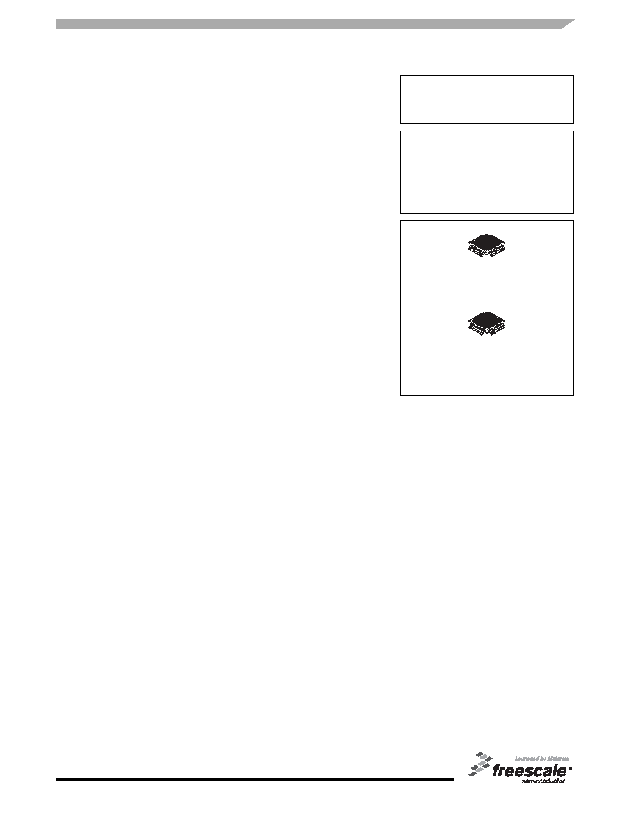
MPC9330
3.3 V 1:6 LVCMOS
PLL CLOCK GENERATOR
FA SUFFIX
32-LEAD LQFP PACKAGE
CASE 873A-03
AC SUFFIX
32-LEAD LQFP PACKAGE
Pb-FREE PACKAGE
CASE 873A-03
相关PDF资料 |
PDF描述 |
|---|---|
| MPC9352FAR2 | 9352 SERIES, PLL BASED CLOCK DRIVER, 11 TRUE OUTPUT(S), 0 INVERTED OUTPUT(S), PQFP32 |
| MPC9352FAR2 | PLL BASED CLOCK DRIVER, 11 TRUE OUTPUT(S), 0 INVERTED OUTPUT(S), PQFP32 |
| MPC9456FA | LOW SKEW CLOCK DRIVER, 10 TRUE OUTPUT(S), 0 INVERTED OUTPUT(S), PQFP32 |
| MPC955FAR2 | 300 MHz, PROC SPECIFIC CLOCK GENERATOR, PQFP32 |
| MPC972FAR2 | 125 MHz, PROC SPECIFIC CLOCK GENERATOR, PQFP52 |
相关代理商/技术参数 |
参数描述 |
|---|---|
| MPC9330FA | 功能描述:时钟发生器及支持产品 3.3V 200MHz Clock Generator RoHS:否 制造商:Silicon Labs 类型:Clock Generators 最大输入频率:14.318 MHz 最大输出频率:166 MHz 输出端数量:16 占空比 - 最大:55 % 工作电源电压:3.3 V 工作电源电流:1 mA 最大工作温度:+ 85 C 安装风格:SMD/SMT 封装 / 箱体:QFN-56 |
| MPC9330FAR2 | 制造商:Integrated Device Technology Inc 功能描述:MPC9330FAR2 - Tape and Reel |
| MPC9331 | 制造商:MOTOROLA 制造商全称:Motorola, Inc 功能描述:3.3 V 1:6 LVCMOS PLL Clock Generator |
| MPC9331AC | 功能描述:时钟发生器及支持产品 FSL1-6 LVCMOS/LVPECL LVCMOS PLL Clk Gen RoHS:否 制造商:Silicon Labs 类型:Clock Generators 最大输入频率:14.318 MHz 最大输出频率:166 MHz 输出端数量:16 占空比 - 最大:55 % 工作电源电压:3.3 V 工作电源电流:1 mA 最大工作温度:+ 85 C 安装风格:SMD/SMT 封装 / 箱体:QFN-56 |
| MPC9331ACR2 | 功能描述:时钟发生器及支持产品 FSL1-6 LVCMOS/LVPECL LVCMOS PLL Clk Gen RoHS:否 制造商:Silicon Labs 类型:Clock Generators 最大输入频率:14.318 MHz 最大输出频率:166 MHz 输出端数量:16 占空比 - 最大:55 % 工作电源电压:3.3 V 工作电源电流:1 mA 最大工作温度:+ 85 C 安装风格:SMD/SMT 封装 / 箱体:QFN-56 |
发布紧急采购,3分钟左右您将得到回复。