- 您现在的位置:买卖IC网 > PDF目录9010 > MPC9330ACR2 (IDT, Integrated Device Technology Inc)IC PLL CLOCK GENERATOR 32-LQFP PDF资料下载
参数资料
| 型号: | MPC9330ACR2 |
| 厂商: | IDT, Integrated Device Technology Inc |
| 文件页数: | 7/13页 |
| 文件大小: | 0K |
| 描述: | IC PLL CLOCK GENERATOR 32-LQFP |
| 标准包装: | 2,000 |
| 类型: | PLL 时钟发生器 |
| PLL: | 带旁路 |
| 输入: | LVCMOS,晶体 |
| 输出: | LVCMOS |
| 电路数: | 1 |
| 比率 - 输入:输出: | 3:6 |
| 差分 - 输入:输出: | 无/无 |
| 频率 - 最大: | 120MHz |
| 除法器/乘法器: | 是/无 |
| 电源电压: | 3.135 V ~ 3.465 V |
| 工作温度: | 0°C ~ 70°C |
| 安装类型: | 表面贴装 |
| 封装/外壳: | 32-LQFP |
| 供应商设备封装: | 32-TQFP(7x7) |
| 包装: | 带卷 (TR) |
MPC9330 REVISION 8 DECEMBER 19, 2012
3
2012 Integrated Device Technology, Inc.
MPC9330 Data Sheet
3.3V, 1:6, LVCMOS PLL CLOCK GENERATOR
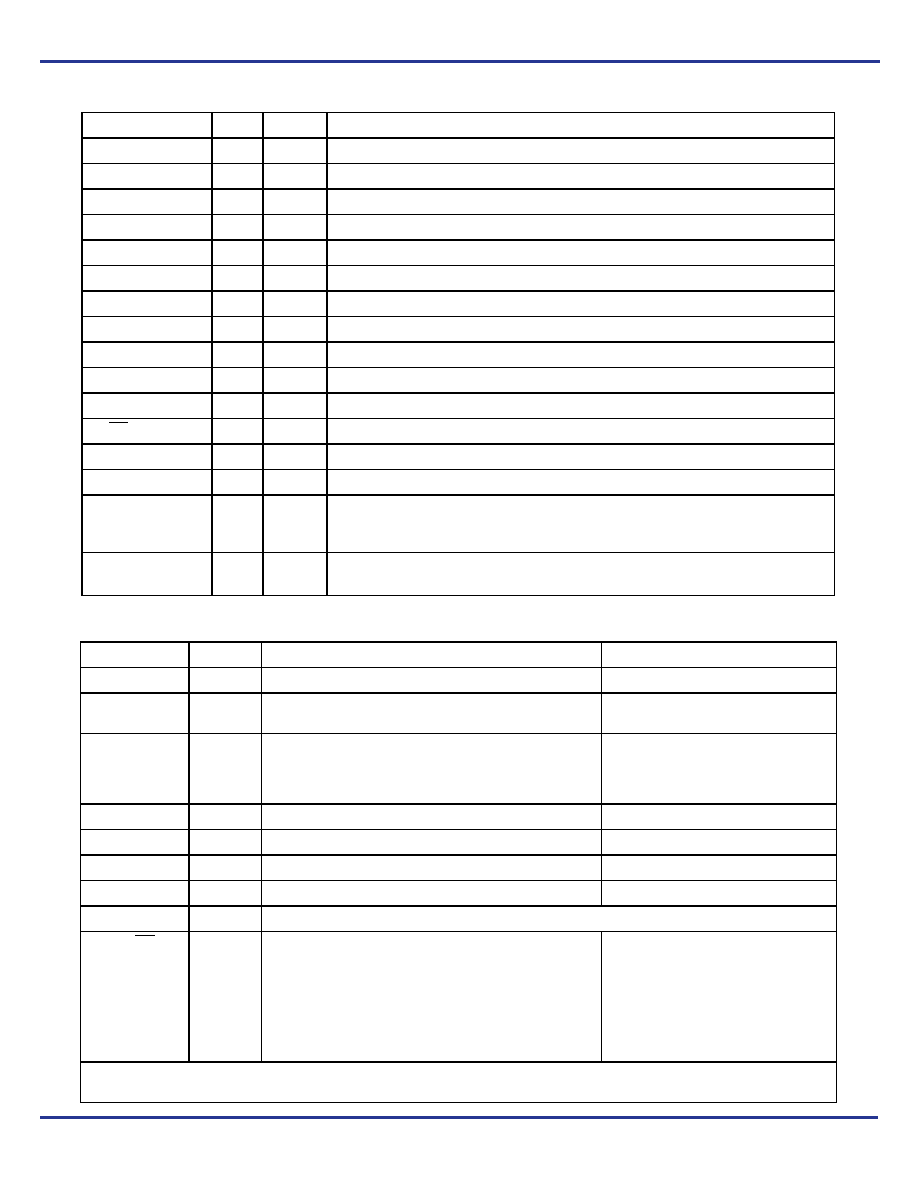
Table 1. Pin Configuration
Pin
I/O
Type
Function
CCLK
Input
LVCMOS
PLL reference clock signal
XTAL_IN, XTAL_OUT
Input
Analog
Crystal oscillator interface
FB_IN
Input
LVCMOS
PLL feedback signal input, connect to an output
FB_SEL
Input
LVCMOS
Feedback select
REF_SEL
Input
LVCMOS
Reference clock select
PWR_DN
Input
LVCMOS
Output frequency and power down select
FSELA
Input
LVCMOS
Frequency divider select for bank A outputs
FSELB
Input
LVCMOS
Frequency divider select for bank B outputs
FSELC
Input
LVCMOS
Frequency divider select for bank C outputs
PLL_EN
Input
LVCMOS
PLL enable/disable
CLK_STOP0-1
Input
LVCMOS
Clock output enable/disable
OE/MR
Input
LVCMOS
Output enable/disable (high-impedance tristate) and device reset
QA0-1, QB0-1, QC0-1
Output
LVCMOS
Clock outputs
GND
Supply Ground
Negative power supply
VCC_PLL
Supply VCC
PLL positive power supply (analog power supply). It is recommended to use an external RC
details.
VCC
Supply VCC
Positive power supply for I/O and core. All VCC pins must be connected to the positive power
supply for correct operation.
Table 2. Function Table
Control
Default
0
1
REF_SEL
0
The crystal oscillator output is the PLL reference clock
CCLK is the PLL reference clock
FB_SEL
0
Internal PLL feedback of 16. fVCO = 16 * fref
External feedback. Zero-delay operation
enabled for CCLK as reference clock
PLL_EN
1
Test mode with PLL disabled. The reference clock is
substituted for the internal VCO output. MPC9330 is fully static
and no minimum frequency limit applies. All PLL related AC
characteristics are not applicable.
Normal operation mode with PLL enabled.
PWR_DN
1
VCO
2 (High output frequency range)
VCO
4 (Low output frequency range)
FSELA
0
Output divider
2
Output divider
4
FSELB
0
Output divider
2
Output divider
4
FSELC
0
Output divider
4
Output divider
6
CLK_STOP[0:1]
11
See Table 3
OE/MR
1
Outputs disabled (high-impedance state) and reset of the
device. During reset in external feedback configuration, the
PLL feedback loop is open. The VCO is tied to its lowest
frequency. The MPC9330 requires reset after any loss of PLL
lock. Loss of PLL lock may occur when the external feedback
path is interrupted. The length of the reset pulse should be
greater than one reference clock cycle (CCLK). Reset does not
affect PLL lock in internal feedback configuration.
Outputs enabled (active)
PWR_DN, FSELA, FSELB and FSELC control the operating PLL frequency range and input/output frequency ratios.
相关PDF资料 |
PDF描述 |
|---|---|
| MS3456KT10SL-3S | CONN PLUG 3POS STRAIGHT W/SCKT |
| MS27484T24F35SD | CONN PLUG 128POS STRAIGHT W/SCKT |
| M83723/73R24576 | CONN RCPT 57POS JAM NUT W/SCKT |
| VE-20Y-MY-F3 | CONVERTER MOD DC/DC 3.3V 33W |
| VI-J7Z-MZ-F2 | CONVERTER MOD DC/DC 2V 10W |
相关代理商/技术参数 |
参数描述 |
|---|---|
| MPC9330FA | 功能描述:时钟发生器及支持产品 3.3V 200MHz Clock Generator RoHS:否 制造商:Silicon Labs 类型:Clock Generators 最大输入频率:14.318 MHz 最大输出频率:166 MHz 输出端数量:16 占空比 - 最大:55 % 工作电源电压:3.3 V 工作电源电流:1 mA 最大工作温度:+ 85 C 安装风格:SMD/SMT 封装 / 箱体:QFN-56 |
| MPC9330FAR2 | 制造商:Integrated Device Technology Inc 功能描述:MPC9330FAR2 - Tape and Reel |
| MPC9331 | 制造商:MOTOROLA 制造商全称:Motorola, Inc 功能描述:3.3 V 1:6 LVCMOS PLL Clock Generator |
| MPC9331AC | 功能描述:时钟发生器及支持产品 FSL1-6 LVCMOS/LVPECL LVCMOS PLL Clk Gen RoHS:否 制造商:Silicon Labs 类型:Clock Generators 最大输入频率:14.318 MHz 最大输出频率:166 MHz 输出端数量:16 占空比 - 最大:55 % 工作电源电压:3.3 V 工作电源电流:1 mA 最大工作温度:+ 85 C 安装风格:SMD/SMT 封装 / 箱体:QFN-56 |
| MPC9331ACR2 | 功能描述:时钟发生器及支持产品 FSL1-6 LVCMOS/LVPECL LVCMOS PLL Clk Gen RoHS:否 制造商:Silicon Labs 类型:Clock Generators 最大输入频率:14.318 MHz 最大输出频率:166 MHz 输出端数量:16 占空比 - 最大:55 % 工作电源电压:3.3 V 工作电源电流:1 mA 最大工作温度:+ 85 C 安装风格:SMD/SMT 封装 / 箱体:QFN-56 |
发布紧急采购,3分钟左右您将得到回复。