- 您现在的位置:买卖IC网 > PDF目录9010 > MPC9330ACR2 (IDT, Integrated Device Technology Inc)IC PLL CLOCK GENERATOR 32-LQFP PDF资料下载
参数资料
| 型号: | MPC9330ACR2 |
| 厂商: | IDT, Integrated Device Technology Inc |
| 文件页数: | 9/13页 |
| 文件大小: | 0K |
| 描述: | IC PLL CLOCK GENERATOR 32-LQFP |
| 标准包装: | 2,000 |
| 类型: | PLL 时钟发生器 |
| PLL: | 带旁路 |
| 输入: | LVCMOS,晶体 |
| 输出: | LVCMOS |
| 电路数: | 1 |
| 比率 - 输入:输出: | 3:6 |
| 差分 - 输入:输出: | 无/无 |
| 频率 - 最大: | 120MHz |
| 除法器/乘法器: | 是/无 |
| 电源电压: | 3.135 V ~ 3.465 V |
| 工作温度: | 0°C ~ 70°C |
| 安装类型: | 表面贴装 |
| 封装/外壳: | 32-LQFP |
| 供应商设备封装: | 32-TQFP(7x7) |
| 包装: | 带卷 (TR) |
MPC9330 REVISION 8 DECEMBER 19, 2012
5
2012 Integrated Device Technology, Inc.
MPC9330 Data Sheet
3.3V, 1:6, LVCMOS PLL CLOCK GENERATOR
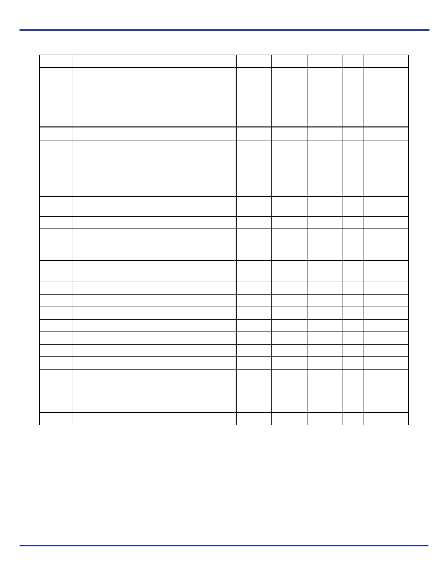
Table 7. AC Characteristics (VCC = 3.3 V 5%, TA = 0°C to 70°C)(1)
1. AC characteristics apply for parallel output termination of 50
to VTT.
Symbol
Characteristics
Min
Typ
Max
Unit
Condition
fref
Input Reference Frequency(2)
4 feedback(3)
PLL mode, external feedback
8 feedback
12 feedback
16 feedback
24 feedback
PLL mode, internal feedback
16 feedback)
Input Reference Frequency in PLL bypass mode(4)
2. PLL mode requires PLL_EN = 0 to enable the PLL.
3.
4 feedback (FB) can be accomplished by setting PWR_DN = 0 and the connection of one 2 output to FB_IN. See Table 3 to Table 5 for
other feedback configurations.
4. In bypass mode, the MPC9330 divides the input reference clock.
50
25
16.67
12.5
8.33
12.5
120
60
40
30
20
30
TBD
MHz
PLL locked
fVCO
VCO Lock Frequency Range(5)
5. The input frequency fref on CCLK must match the VCO frequency range divided by the feedback divider ratio FB: fref = fVCO FB.
200
480
MHz
fXTAL
Crystal Interface Frequency Range(6)
6. The usable crystal frequency range depends on the VCO lock frequency and the PLL feedback ratio.
10
25
MHz
fMAX
Output Frequency
4 output
8 output
12 output
16 output
24 output
50
25
16.67
12.5
8.33
120
60
40
30
20
MHz
PLL locked
frefDC
tPW, MIN
Reference Input Duty Cycle
Minimum Input Reference Pulse Width
25
2
75
%
ns
tr, tf
CCLK Input Rise/Fall Time
1.0
ns
0.8 to 2.0 V
t()
Propagation Delay (SPO)(7) for the
- entire fref range
- fref = 8.33 MHz
- fref = 50.0 MHz
7. SPO is the static phase offset between CCLK and FB_IN (FB_SEL=1 and PLL locked). tsk(o) [ps] = tsk(o) [°] B(fref 360°)
-1.2
-400
-70
+1.2
+400
+70
°
ps
tsk(o)
Output-to-Output Skew(8)
(within output bank)
(any output)
8. Skew data applicable for equally loaded outputs only.
50
150
ps
DC
Output Duty Cycle
45
50
55
%
tr, tf
Output Rise/Fall Time
0.1
1.0
ns
0.55 to 2.4 V
tPLZ, HZ
Output Disable Time
10
ns
tPZL, LZ
Output Enable Time
10
ns
tJIT(CC)
Cycle-to-cycle jitter
50
300
ps
tJIT(PER)
Period Jitter
35
250
ps
tJIT()
I/O Phase Jitter
RMS (1
)
10
70
ps
BW
PLL closed loop bandwidth(9)
4 feedback
PLL mode, external feedback
8 feedback
12 feedback
16 feedback
24 feedback
9. –3 dB point of PLL transfer characteristics.
0.8-5.0
0.5-2.0
0.3-1.0
0.25-0.6
0.2-0.5
MHz
tLOCK
Maximum PLL Lock Time
10
ms
相关PDF资料 |
PDF描述 |
|---|---|
| MS3456KT10SL-3S | CONN PLUG 3POS STRAIGHT W/SCKT |
| MS27484T24F35SD | CONN PLUG 128POS STRAIGHT W/SCKT |
| M83723/73R24576 | CONN RCPT 57POS JAM NUT W/SCKT |
| VE-20Y-MY-F3 | CONVERTER MOD DC/DC 3.3V 33W |
| VI-J7Z-MZ-F2 | CONVERTER MOD DC/DC 2V 10W |
相关代理商/技术参数 |
参数描述 |
|---|---|
| MPC9330FA | 功能描述:时钟发生器及支持产品 3.3V 200MHz Clock Generator RoHS:否 制造商:Silicon Labs 类型:Clock Generators 最大输入频率:14.318 MHz 最大输出频率:166 MHz 输出端数量:16 占空比 - 最大:55 % 工作电源电压:3.3 V 工作电源电流:1 mA 最大工作温度:+ 85 C 安装风格:SMD/SMT 封装 / 箱体:QFN-56 |
| MPC9330FAR2 | 制造商:Integrated Device Technology Inc 功能描述:MPC9330FAR2 - Tape and Reel |
| MPC9331 | 制造商:MOTOROLA 制造商全称:Motorola, Inc 功能描述:3.3 V 1:6 LVCMOS PLL Clock Generator |
| MPC9331AC | 功能描述:时钟发生器及支持产品 FSL1-6 LVCMOS/LVPECL LVCMOS PLL Clk Gen RoHS:否 制造商:Silicon Labs 类型:Clock Generators 最大输入频率:14.318 MHz 最大输出频率:166 MHz 输出端数量:16 占空比 - 最大:55 % 工作电源电压:3.3 V 工作电源电流:1 mA 最大工作温度:+ 85 C 安装风格:SMD/SMT 封装 / 箱体:QFN-56 |
| MPC9331ACR2 | 功能描述:时钟发生器及支持产品 FSL1-6 LVCMOS/LVPECL LVCMOS PLL Clk Gen RoHS:否 制造商:Silicon Labs 类型:Clock Generators 最大输入频率:14.318 MHz 最大输出频率:166 MHz 输出端数量:16 占空比 - 最大:55 % 工作电源电压:3.3 V 工作电源电流:1 mA 最大工作温度:+ 85 C 安装风格:SMD/SMT 封装 / 箱体:QFN-56 |
发布紧急采购,3分钟左右您将得到回复。