- 您现在的位置:买卖IC网 > PDF目录2014 > MPC93H51AC (IDT, Integrated Device Technology Inc)IC PLL CLK DRIVER LV 32-LQFP PDF资料下载
参数资料
| 型号: | MPC93H51AC |
| 厂商: | IDT, Integrated Device Technology Inc |
| 文件页数: | 13/14页 |
| 文件大小: | 0K |
| 描述: | IC PLL CLK DRIVER LV 32-LQFP |
| 标准包装: | 250 |
| 类型: | PLL 时钟发生器 |
| PLL: | 带旁路 |
| 输入: | LVCMOS,LVPECL |
| 输出: | LVCMOS |
| 电路数: | 1 |
| 比率 - 输入:输出: | 2:11 |
| 差分 - 输入:输出: | 是/无 |
| 频率 - 最大: | 240MHz |
| 除法器/乘法器: | 是/无 |
| 电源电压: | 3.135 V ~ 3.465 V |
| 工作温度: | 0°C ~ 70°C |
| 安装类型: | 表面贴装 |
| 封装/外壳: | 32-LQFP |
| 供应商设备封装: | 32-TQFP(7x7) |
| 包装: | 托盘 |
MPC93H51 REVISION 4 FEBRUARY 15, 2013
8
2013 Integrated Device Technology, Inc.
MPC93H51 Data Sheet
LOW VOLTAGE PLL CLOCK DRIVER
provides separate power supplies for the output buffers (VCC)
and the phase-locked loop (VCCA) of the device.The purpose
of this design technique is to isolate the high switching noise
digital outputs from the relatively sensitive internal analog
phase-locked loop. In a digital system environment where it
is more difficult to minimize noise on the power supplies, a
second level of isolation may be required. The simple but
effective form of isolation is a power supply filter on the VCCA
pin for the MPC93H51.
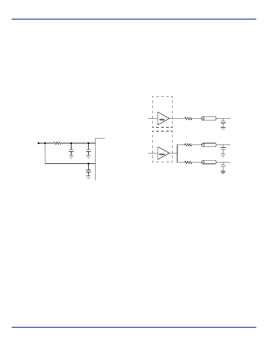
Figure 6 illustrates a typical power supply filter scheme.
The MPC93H51 frequency and phase stability is most
susceptible to noise with spectral content in the 100 kHz to 20
MHz range; therefore, the filter should be designed to target
this range. The key parameter that needs to be met in the
final filter design is the DC voltage drop across the series filter
resistor RF. From the data sheet the ICCA current (the current
sourced through the VCCA pin) is typically 6 mA (12 mA
maximum), assuming that a minimum of 3.0 V must be
maintained on the VCCA pin. The resistor RF shown
in Figure 6 must have a resistance of 5–15
to meet the
voltage drop criteria.
Figure 6. VCCA Power Supply Filter
As the noise frequency crosses the series resonant point
of an individual capacitor, its overall impedance begins to
look inductive and thus increases with increasing frequency.
The parallel capacitor combination shown ensures that a low
impedance path to ground exists for frequencies well above
the bandwidth of the PLL. Although the MPC93H51 has
several design features to minimize the susceptibility to
power supply noise (isolated power and grounds and fully
differential PLL), there still may be applications in which
overall performance is being degraded due to system power
supply noise. The power supply filter schemes discussed in
this section should be adequate to eliminate power supply
noise related problems in most designs.
Driving Transmission Lines
The MPC93H51 clock driver was designed to drive high
speed signals in a terminated transmission line environment.
To provide the optimum flexibility to the user, the output
drivers were designed to exhibit the lowest impedance
possible. With an output impedance of less than 20
the
drivers can drive either parallel or series terminated
transmission lines. For more information on transmission
lines the reader is referred to Freescale application note
AN1091. In most high performance clock networks,
point-to-point distribution of signals is the method of choice.
In a point-to-point scheme, either series terminated or parallel
terminated transmission lines can be used. The parallel
technique terminates the signal at the end of the line with a
50
resistance to VCC 2.
This technique draws a fairly high level of DC current and
thus only a single terminated line can be driven by each
output of the MPC93H51 clock driver. For the series
terminated case, however, there is no DC current draw; thus,
the outputs can drive multiple series terminated lines.
Figure 7 illustrates an output driving a single series
terminated line versus two series terminated lines in parallel.
When taken to its extreme the fanout of the MPC93H51 clock
driver is effectively doubled due to its capability to drive
multiple lines.
Figure 7. Single versus Dual Transmission Lines
The waveform plots in Figure 8 show the simulation results
of an output driving a single line versus two lines. In both
cases, the drive capability of the MPC93H51 output buffer is
more than sufficient to drive 50
transmission lines on the
incident edge. Note from the delay measurements in the
simulations, a delta of only 43 ps exists between the two
differently loaded outputs. This suggests that the dual line
driving need not be used exclusively to maintain the tight
output-to-output skew of the MPC93H51. The output
waveform in Figure 8 shows a step in the waveform. This
step is caused by the impedance mismatch seen looking into
the driver. The parallel combination of the 36
series resistor
plus the output impedance does not match the parallel
combination of the line impedances. The voltage wave
launched down the two lines will equal:
VL =VS (Z0 (RS + R0 + Z0))
Z0 =50 || 50
RS =36 || 36
R0 =14
VL = 3.0 (25 (18 + 17 + 25)
= 1.31 V
At the load end, the voltage will double to 2.6 V due to the
near unity reflection coefficient. It will then increment towards
the quiescent 3.0 V in steps separated by one round trip delay
(in this case 4.0 ns).
VCCA
VCC
MPC93H51
0.01
F
22
F
RF
VCC
0.01
F
10
IN
MPC93H51
Output
Buffer
RS = 36
ZO = 50
OutA
10
IN
MPC93H51
Output
Buffer
RS = 36
ZO = 50
OutB0
RS = 36
ZO = 50
OutB1
相关PDF资料 |
PDF描述 |
|---|---|
| MPC93H52AC | IC CLK GEN ZD 1:11 32-LQFP |
| MPC93R51AC | IC PLL CLK DRIVER LV 32-LQFP |
| MPC9608AC | IC CLOCK BUFFER ZD 1:10 32-LQFP |
| MPC962309EJ-1H | IC BUFFER ZD 1:5 3.3V 16-TSSOP |
| MPC96877VK | IC CLK DRIVER 1:10 SDRAM 52-BGA |
相关代理商/技术参数 |
参数描述 |
|---|---|
| MPC93H51ACR2 | 功能描述:时钟发生器及支持产品 FSL 1-9 LVCMOS/LVPEC L to LVCMOS PLL Cloc RoHS:否 制造商:Silicon Labs 类型:Clock Generators 最大输入频率:14.318 MHz 最大输出频率:166 MHz 输出端数量:16 占空比 - 最大:55 % 工作电源电压:3.3 V 工作电源电流:1 mA 最大工作温度:+ 85 C 安装风格:SMD/SMT 封装 / 箱体:QFN-56 |
| MPC93H51FA | 功能描述:IC PLL CLK DVR HI-DRIVE 32-LQFP RoHS:否 类别:集成电路 (IC) >> 时钟/计时 - 时钟发生器,PLL,频率合成器 系列:- 标准包装:39 系列:- 类型:* PLL:带旁路 输入:时钟 输出:时钟 电路数:1 比率 - 输入:输出:1:10 差分 - 输入:输出:是/是 频率 - 最大:170MHz 除法器/乘法器:无/无 电源电压:2.375 V ~ 3.465 V 工作温度:0°C ~ 70°C 安装类型:* 封装/外壳:* 供应商设备封装:* 包装:* |
| MPC93H52AC | 功能描述:时钟发生器及支持产品 FSL 1-11 LVCMOS PLL Clock Generator, hig RoHS:否 制造商:Silicon Labs 类型:Clock Generators 最大输入频率:14.318 MHz 最大输出频率:166 MHz 输出端数量:16 占空比 - 最大:55 % 工作电源电压:3.3 V 工作电源电流:1 mA 最大工作温度:+ 85 C 安装风格:SMD/SMT 封装 / 箱体:QFN-56 |
| MPC93H52ACR2 | 功能描述:IC CLK GEN ZD 1:11 32-LQFP RoHS:是 类别:集成电路 (IC) >> 时钟/计时 - 时钟发生器,PLL,频率合成器 系列:- 标准包装:1,000 系列:- 类型:时钟/频率合成器,扇出分配 PLL:- 输入:- 输出:- 电路数:- 比率 - 输入:输出:- 差分 - 输入:输出:- 频率 - 最大:- 除法器/乘法器:- 电源电压:- 工作温度:- 安装类型:表面贴装 封装/外壳:56-VFQFN 裸露焊盘 供应商设备封装:56-VFQFP-EP(8x8) 包装:带卷 (TR) 其它名称:844S012AKI-01LFT |
| MPC93H52FA | 功能描述:IC CLOCK GEN/DVR HI-DRIVE 32LQFP RoHS:否 类别:集成电路 (IC) >> 时钟/计时 - 时钟发生器,PLL,频率合成器 系列:- 标准包装:39 系列:- 类型:* PLL:带旁路 输入:时钟 输出:时钟 电路数:1 比率 - 输入:输出:1:10 差分 - 输入:输出:是/是 频率 - 最大:170MHz 除法器/乘法器:无/无 电源电压:2.375 V ~ 3.465 V 工作温度:0°C ~ 70°C 安装类型:* 封装/外壳:* 供应商设备封装:* 包装:* |
发布紧急采购,3分钟左右您将得到回复。