- 您现在的位置:买卖IC网 > PDF目录29137 > MPC93R51FAR2 (FREESCALE SEMICONDUCTOR INC) 93R SERIES, PLL BASED CLOCK DRIVER, 9 TRUE OUTPUT(S), 0 INVERTED OUTPUT(S), PQFP32 PDF资料下载
参数资料
| 型号: | MPC93R51FAR2 |
| 厂商: | FREESCALE SEMICONDUCTOR INC |
| 元件分类: | 时钟及定时 |
| 英文描述: | 93R SERIES, PLL BASED CLOCK DRIVER, 9 TRUE OUTPUT(S), 0 INVERTED OUTPUT(S), PQFP32 |
| 封装: | 7 X 7 MM, PLASTIC, LQFP-32 |
| 文件页数: | 5/9页 |
| 文件大小: | 336K |
| 代理商: | MPC93R51FAR2 |
MPC93R51
MOTOROLA ADVANCED CLOCK DRIVERS DEVICE DATA
134
APPLICATIONS INFORMATION
Programming the MPC93R51
The MPC93R51 clock driver outputs can be configured into
several divider modes, in addition the external feedback of the
device allows for flexibility in establishing various input to out-
put frequency relationships. The output divider of the four out-
put groups allows the user to configure the outputs into 1:1,
2:1, 4:1 and 4:2:1 frequency ratios. The use of even dividers
ensure that the output duty cycle is always 50%. “Output Fre-
quency Relationship for an Example Configuration” illustrates
the various output configurations, the table describes the out-
puts using the input clock frequency CLK as a reference.
The output division settings establish the output relation-
ship, in addition, it must be ensured that the VCO will be stable
given the frequency of the outputs desired. The feedback fre-
quency should be used to situate the VCO into a frequency
range in which the PLL will be stable. The design of the PLL
supports output frequencies from 25 MHz to 240 MHz while the
VCO frequency range is specified from 200 MHz to 480 MHz
and should not be exceeded for stable operation.
Output Frequency Relationshipa for an Example Configuration
Inputs
Outputs
FSELA
FSELB
FSELC
FSELD
QA
QB
QC
QD
0
2 * CLK
CLK
0
1
2 * CLK
CLK
÷ 2
0
1
0
4 * CLK
2 * CLK
CLK
2* CLK
0
1
4 * CLK
2 * CLK
CLK
0
1
0
2 * CLK
CLK
÷ 2
CLK
0
1
0
1
2 * CLK
CLK
÷ 2
CLK
÷ 2
0
1
0
4 * CLK
CLK
2 * CLK
0
1
4 * CLK
CLK
1
0
CLK
1
0
1
CLK
÷ 2
1
0
1
0
2 * CLK
CLK
2 * CLK
1
0
1
2 * CLK
CLK
1
0
CLK
÷ 2
CLK
1
0
1
CLK
÷ 2
CLK
÷ 2
1
0
2 * CLK
CLK
2 * CLK
1
2 * CLK
CLK
a. Output frequency relationship with respect to input reference frequency CLK. QC1 is connected to EXT_FB.
Using the MPC93R51 in zero–delay applications
Nested clock trees are typical applications for the
MPC93R51. For these applications the MPC93R51 offers a
differential LVPECL clock input pair as a PLL reference. This
allows for the use of differential LVPECL primary clock distribu-
tion devices such as the Motorola MC100EP111 or
MC10EP222, taking advantage of its superior low-skew perfor-
mance. Clock trees using LVPECL for clock distribution and
the MPC93R51 as LVCMOS PLL fanout buffer with zero inser-
tion delay will show significantly lower clock skew than clock
distributions developed from CMOS fanout buffers.
The external feedback option of the MPC93R51 PLL allows
for its use as a zero delay buffer. The PLL aligns the feedback
clock output edge with the clock input reference edge and
virtually eliminates the propagation delay through the device.
The remaining insertion delay (skew error) of the
MPC93R51 in zero-delay applications is measured between
the reference clock input and any output. This effective delay
consists of the static phase offset (SPO or t()), I/O jitter
(tJIT(), phase or long-term jitter), feedback path delay and the
output-to-output skew (tSK(O) relative to the feedback output.
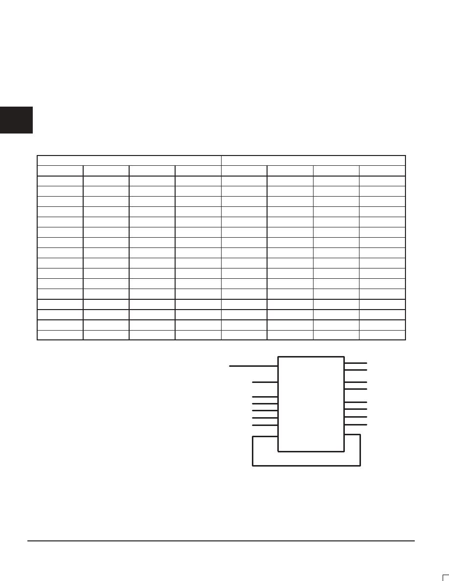
MPC93R51 zero–delay configuration (feedback of QD4)
MPC93R51
TCLK
QA
fref = 100 MHz
REF_SEL
PLL_EN
FSELA
FSELB
FSELC
FSELD
Ext_FB
QB
QC0
QC1
QD0
QD1
QD2
QD3
QD4
2 x 100 MHz
4 x 100 MHz
100 MHz (Feedback)
1
0
Calculation of part-to-part skew
The MPC93R51 zero delay buffer supports applications
where critical clock signal timing can be maintained across
several devices. If the reference clock inputs (TCLK or PCLK)
of two or more MPC93R51 are connected together, the maxi-
2
F
re
e
sc
a
le
S
e
m
ic
o
n
d
u
c
to
r,
I
Freescale Semiconductor, Inc.
For More Information On This Product,
Go to: www.freescale.com
n
c
..
.
相关PDF资料 |
PDF描述 |
|---|---|
| MPC93R51FA | 93R SERIES, PLL BASED CLOCK DRIVER, 9 TRUE OUTPUT(S), 0 INVERTED OUTPUT(S), PQFP32 |
| MPC93R51ACR2 | 93R SERIES, PLL BASED CLOCK DRIVER, 9 TRUE OUTPUT(S), 0 INVERTED OUTPUT(S), PQFP32 |
| MPC940LFAR2 | MPC900 SERIES, LOW SKEW CLOCK DRIVER, 18 TRUE OUTPUT(S), 0 INVERTED OUTPUT(S), PQFP32 |
| MPC940LFA | MPC900 SERIES, LOW SKEW CLOCK DRIVER, 18 TRUE OUTPUT(S), 0 INVERTED OUTPUT(S), PQFP32 |
| MPC942PFAR2 | 942 SERIES, LOW SKEW CLOCK DRIVER, 18 TRUE OUTPUT(S), 0 INVERTED OUTPUT(S), PQFP32 |
相关代理商/技术参数 |
参数描述 |
|---|---|
| MPC93R52 | 制造商:MOTOROLA 制造商全称:Motorola, Inc 功能描述:LOW VOLTAGE 3.3V LVCMOS 1:11 CLOCK GENERATOR |
| MPC93R52AC | 功能描述:时钟发生器及支持产品 FSL 1-11 LVCMOS PLL Clock Generator, pwr RoHS:否 制造商:Silicon Labs 类型:Clock Generators 最大输入频率:14.318 MHz 最大输出频率:166 MHz 输出端数量:16 占空比 - 最大:55 % 工作电源电压:3.3 V 工作电源电流:1 mA 最大工作温度:+ 85 C 安装风格:SMD/SMT 封装 / 箱体:QFN-56 |
| MPC93R52ACR2 | 功能描述:时钟发生器及支持产品 FSL 1-11 LVCMOS PLL Clock Generator, pwr RoHS:否 制造商:Silicon Labs 类型:Clock Generators 最大输入频率:14.318 MHz 最大输出频率:166 MHz 输出端数量:16 占空比 - 最大:55 % 工作电源电压:3.3 V 工作电源电流:1 mA 最大工作温度:+ 85 C 安装风格:SMD/SMT 封装 / 箱体:QFN-56 |
| MPC93R52FA | 功能描述:时钟发生器及支持产品 3.3V 240MHz Clock Generator RoHS:否 制造商:Silicon Labs 类型:Clock Generators 最大输入频率:14.318 MHz 最大输出频率:166 MHz 输出端数量:16 占空比 - 最大:55 % 工作电源电压:3.3 V 工作电源电流:1 mA 最大工作温度:+ 85 C 安装风格:SMD/SMT 封装 / 箱体:QFN-56 |
| MPC93R52FAR2 | 制造商:Integrated Device Technology Inc 功能描述:Zero Delay PLL Clock Generator Single 32-Pin LQFP T/R 制造商:Integrated Device Technology Inc 功能描述:ZERO DLY PLL CLOCK GEN SGL 32LQFP - Tape and Reel |
发布紧急采购,3分钟左右您将得到回复。