- 您现在的位置:买卖IC网 > PDF目录2014 > MPC9608AC (IDT, Integrated Device Technology Inc)IC CLOCK BUFFER ZD 1:10 32-LQFP PDF资料下载
参数资料
| 型号: | MPC9608AC |
| 厂商: | IDT, Integrated Device Technology Inc |
| 文件页数: | 11/13页 |
| 文件大小: | 0K |
| 描述: | IC CLOCK BUFFER ZD 1:10 32-LQFP |
| 标准包装: | 250 |
| 类型: | 零延迟缓冲器 |
| PLL: | 带旁路 |
| 输入: | LVCMOS |
| 输出: | LVCMOS |
| 电路数: | 1 |
| 比率 - 输入:输出: | 1:10 |
| 差分 - 输入:输出: | 无/无 |
| 频率 - 最大: | 200MHz |
| 除法器/乘法器: | 是/无 |
| 电源电压: | 3.135 V ~ 3.465 V |
| 工作温度: | -40°C ~ 85°C |
| 安装类型: | 表面贴装 |
| 封装/外壳: | 32-LQFP |
| 供应商设备封装: | 32-TQFP(7x7) |
| 包装: | 托盘 |
MPC9608 REVISION 4 JANUARY 7, 2013
7
2013 Integrated Device Technology, Inc.
MPC9608 Data Sheet
1:10 LVCMOS ZERO DELAY CLOCK BUFFER
Due to the statistical nature of I/O jitter, an RMS value (1
)
is specified. I/O jitter numbers for other confidence factors
(CF) can be derived from Table 8.
The feedback trace delay is determined by the board
layout and can be used to fine-tune the effective delay
through each device. In the following example calculation a
I/O jitter confidence factor of 99.7% (
3) is assumed,
resulting in a worst case timing uncertainty from input to any
output of -295 ps to 295 ps(1) relative to CCLK:
tSK(PP) = [-100 ps...100 ps] + [-150 ps...150 ps] +
[(15 ps -3)...(15 ps 3)] + tPD, LINE(FB)
tSK(PP) = [-295 ps...295 ps] + tPD, LINE(FB)
Driving Transmission Lines
The MPC9608 clock driver was designed to drive high
speed signals in a terminated transmission line environment.
To provide the optimum flexibility to the user the output driv-
ers were designed to exhibit the lowest impedance possible.
With an output impedance of less than 20
the drivers can
drive either parallel or series terminated transmission lines.
For more information on transmission lines the reader is re-
ferred to Freescale Semiconductor application note AN1091.
In most high performance clock networks point-to-point distri-
bution of signals is the method of choice. In a point-to-point
scheme either series terminated or parallel terminated trans-
mission lines can be used. The parallel technique terminates
the signal at the end of the line with a 50
resistance to
VCC 2.
This technique draws a fairly high level of DC current and
thus only a single terminated line can be driven by each
output of the MPC9608 clock driver. For the series terminated
case however there is no DC current draw, thus the outputs
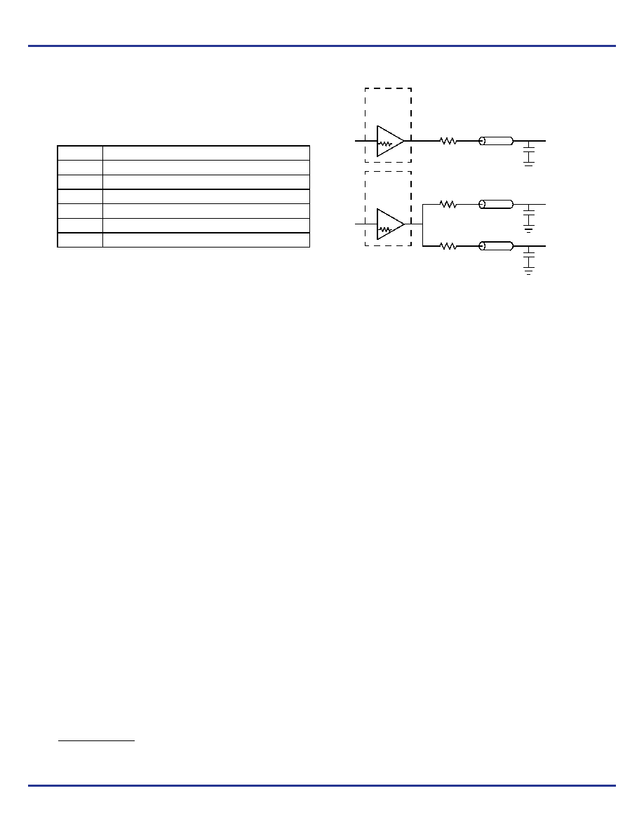
can drive multiple series terminated lines. Figure 5 illustrates
an output driving a single series terminated line versus two
series terminated lines in parallel. When taken to its extreme,
the fanout of the MPC9608 clock driver is effectively doubled
due to its capability to drive multiple lines.
Figure 5. Single versus Dual Transmission Lines
The waveform plots in Figure 6. Single versus Dual
Waveforms show the simulation results of an output driving a
single line versus two lines. In both cases the drive capability
of the MPC9608 output buffer is more than sufficient to drive
50
transmission lines on the incident edge. From the delay
measurements in the simulations a delta of only 43 ps exists
between the two differently loaded outputs. This suggests
that the dual line driving need not be used exclusively to
maintain the tight output-to-output skew of the MPC9608.
The output waveform in Figure 6. Single versus Dual
Waveforms shows a step in the waveform. This step is
caused by the impedance mismatch seen looking into the
driver. The parallel combination of the 36
series resistor
plus the output impedance does not match the parallel
combination of the line impedances. The voltage wave
launched down the two lines will equal:
VL =VS (Z0 (RS +R0 +Z0))
Z0 =50 || 50
RS =36 || 36
R0 =14
VL = 3.0 (25 (18 + 17 + 25))
=1.31 V
At the load end the voltage will double to 2.6 V due to the
near unity reflection coefficient. It will then increment towards
the quiescent 3.0 V in steps separated by one round trip delay
(in this case 4.0 ns).
Table 8. Confidence Factor CF
CF
Probability of clock edge within the distribution
1
0.68268948
2
0.95449988
3
0.99730007
4
0.99993663
5
0.99999943
6
0.99999999
1. Skew data are designed targets and pending device specifications.
14
IN
MPC9608
Output
Buffer
RS = 36
ZO = 50
OutA
14
IN
MPC9608
Output
Buffer
RS = 36
ZO = 50
OutB0
RS = 36
ZO = 50
OutB1
相关PDF资料 |
PDF描述 |
|---|---|
| MPC962309EJ-1H | IC BUFFER ZD 1:5 3.3V 16-TSSOP |
| MPC96877VK | IC CLK DRIVER 1:10 SDRAM 52-BGA |
| MPC9773AE | IC PLL CLK GEN 1:12 3.3V 52-LQFP |
| MPC9850VF | IC PLL CLOCK GENERATOR 100MAPBGA |
| MPC9855VM | IC PLL CLOCK GENERATOR 100MAPBGA |
相关代理商/技术参数 |
参数描述 |
|---|---|
| MPC9608ACR2 | 功能描述:时钟缓冲器 RoHS:否 制造商:Texas Instruments 输出端数量:5 最大输入频率:40 MHz 传播延迟(最大值): 电源电压-最大:3.45 V 电源电压-最小:2.375 V 最大功率耗散: 最大工作温度:+ 85 C 最小工作温度:- 40 C 封装 / 箱体:LLP-24 封装:Reel |
| MPC9608FA | 功能描述:时钟缓冲器 3.3V 200MHz Clock Generator RoHS:否 制造商:Texas Instruments 输出端数量:5 最大输入频率:40 MHz 传播延迟(最大值): 电源电压-最大:3.45 V 电源电压-最小:2.375 V 最大功率耗散: 最大工作温度:+ 85 C 最小工作温度:- 40 C 封装 / 箱体:LLP-24 封装:Reel |
| MPC9608FAR2 | 制造商:Integrated Device Technology Inc 功能描述:ZERO DLY PLL CLOCK BFFR SGL 32LQFP - Tape and Reel |
| MPC961C | 制造商:MOTOROLA 制造商全称:Motorola, Inc 功能描述:LOW VOLTAGE ZERO DELAY BUFFER |
| MPC961CAC | 功能描述:时钟缓冲器 RoHS:否 制造商:Texas Instruments 输出端数量:5 最大输入频率:40 MHz 传播延迟(最大值): 电源电压-最大:3.45 V 电源电压-最小:2.375 V 最大功率耗散: 最大工作温度:+ 85 C 最小工作温度:- 40 C 封装 / 箱体:LLP-24 封装:Reel |
发布紧急采购,3分钟左右您将得到回复。