- 您现在的位置:买卖IC网 > PDF目录29137 > MPC9658FA (FREESCALE SEMICONDUCTOR INC) 9658 SERIES, PLL BASED CLOCK DRIVER, 10 TRUE OUTPUT(S), 0 INVERTED OUTPUT(S), PQFP32 PDF资料下载
参数资料
| 型号: | MPC9658FA |
| 厂商: | FREESCALE SEMICONDUCTOR INC |
| 元件分类: | 时钟及定时 |
| 英文描述: | 9658 SERIES, PLL BASED CLOCK DRIVER, 10 TRUE OUTPUT(S), 0 INVERTED OUTPUT(S), PQFP32 |
| 封装: | 7 X 7 MM, LQFP-32 |
| 文件页数: | 6/12页 |
| 文件大小: | 344K |
| 代理商: | MPC9658FA |
Advanced Clock Drivers Device Data
Freescale Semiconductor
3
MPC9658
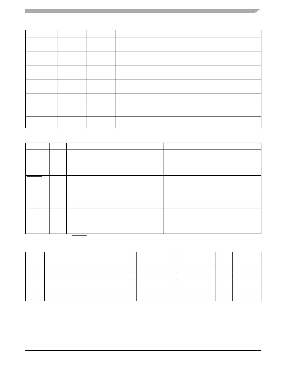
Table 1. Pin Configurations
Number
Name
Type
Description
PCLK, PCLK
Input
LVPECL
PECL reference clock signal
FB_IN
Input
LVCMOS
PLL feedback signal input, connect to QFB
VCO_SEL
Input
LVCMOS
Operating frequency range select
BYPASS
Input
LVCMOS
PLL and output divider bypass select
PLL_EN
Input
LVCMOS
PLL enable/disable
MR/OE
Input
LVCMOS
Output enable/disable (high-impedance tristate) and device reset
Q0–9
Output
LVCMOS
Clock outputs
QFB
Output
LVCMOS
Clock output for PLL feedback, connect to FB_IN
GND
Supply
Ground
Negative power supply (GND)
VCC_PLL
Supply
VCC
PLL positive power supply (analog power supply). It is recommended to use an external
INFORMATION for details.
VCC
Supply
VCC
Positive power supply for I/O and core. All VCC pins must be connected to the positive
power supply for correct operation.
Table 2. Function Table
Control
Default
0
1
PLL_EN
1
Test mode with PLL bypassed. The reference clock
(PCLK) is substituted for the internal VCO output.
MPC9658 is fully static and no minimum frequency limit
applies. All PLL related AC characteristics are not
applicable.
Selects the VCO output.(1)
1. PLL operation requires BYPASS = 1 and PLL_EN = 1.
BYPASS
1
Test mode with PLL and output dividers bypassed. The
reference clock (PCLK) is directly routed to the outputs.
MPC9658 is fully static and no minimum frequency limit
applies. All PLL related AC characteristics are not
applicable.
Selects the output dividers.
VCO_SEL
1
VCO
÷ 1 (High frequency range). fREF = fQ0–9 = 2 fVCO
VCO
÷ 2 (Low output range). fREF = fQ0–9 = 4 fVCO
MR/OE
0
Outputs enabled (active)
Outputs disabled (high-impedance state) and reset of the
device. During reset the PLL feedback loop is open. The
VCO is tied to its lowest frequency. The length of the reset
pulse should be greater than one reference clock cycle
(PCLK).
Table 3. Absolute Maximum Ratings(1)
1. Absolute maximum continuous ratings are those maximum values beyond which damage to the device may occur. Exposure to these
conditions or conditions beyond those indicated may adversely affect device reliability. Functional operation at absolute-maximum-rated
conditions is not implied.
Symbol
Characteristics
Min
Max
Unit
Condition
VCC
Supply Voltage
–0.3
3.9
V
VIN
DC Input Voltage
–0.3
VCC +0.3
V
VOUT
DC Output Voltage
–0.3
VCC +0.3
V
IIN
DC Input Current
±20
mA
IOUT
DC Output Current
±50
mA
TS
Storage Temperature
–65
125
°C
相关PDF资料 |
PDF描述 |
|---|---|
| MPC9658ACR2 | 9658 SERIES, PLL BASED CLOCK DRIVER, 10 TRUE OUTPUT(S), 0 INVERTED OUTPUT(S), PQFP32 |
| MPC973FA | 973 SERIES, PLL BASED CLOCK DRIVER, 12 TRUE OUTPUT(S), 0 INVERTED OUTPUT(S), PQFP52 |
| MPC974FAR2 | 974 SERIES, PLL BASED CLOCK DRIVER, 14 TRUE OUTPUT(S), 0 INVERTED OUTPUT(S), PQFP52 |
| MPC974FA | 974 SERIES, PLL BASED CLOCK DRIVER, 14 TRUE OUTPUT(S), 0 INVERTED OUTPUT(S), PQFP52 |
| MPC974FA | 974 SERIES, PLL BASED CLOCK DRIVER, 14 TRUE OUTPUT(S), 0 INVERTED OUTPUT(S), PQFP52 |
相关代理商/技术参数 |
参数描述 |
|---|---|
| MPC9658FAR2 | 制造商:Integrated Device Technology Inc 功能描述:PLL Clock Driver Single 32-Pin LQFP T/R 制造商:Integrated Device Technology Inc 功能描述:MPC9658FAR2 - Tape and Reel |
| MPC96877VK | 功能描述:时钟发生器及支持产品 DDR2 PLL RoHS:否 制造商:Silicon Labs 类型:Clock Generators 最大输入频率:14.318 MHz 最大输出频率:166 MHz 输出端数量:16 占空比 - 最大:55 % 工作电源电压:3.3 V 工作电源电流:1 mA 最大工作温度:+ 85 C 安装风格:SMD/SMT 封装 / 箱体:QFN-56 |
| MPC96877VKR2 | 功能描述:时钟发生器及支持产品 DDR2 PLL RoHS:否 制造商:Silicon Labs 类型:Clock Generators 最大输入频率:14.318 MHz 最大输出频率:166 MHz 输出端数量:16 占空比 - 最大:55 % 工作电源电压:3.3 V 工作电源电流:1 mA 最大工作温度:+ 85 C 安装风格:SMD/SMT 封装 / 箱体:QFN-56 |
| MPC970 | 制造商:MOTOROLA 制造商全称:Motorola, Inc 功能描述:LOW VOLTAGE PLL CLOCK DRIVER |
| MPC972 | 制造商:Motorola Inc 功能描述: |
发布紧急采购,3分钟左右您将得到回复。