- 您现在的位置:买卖IC网 > PDF目录29137 > MPC9658FA (FREESCALE SEMICONDUCTOR INC) 9658 SERIES, PLL BASED CLOCK DRIVER, 10 TRUE OUTPUT(S), 0 INVERTED OUTPUT(S), PQFP32 PDF资料下载
参数资料
| 型号: | MPC9658FA |
| 厂商: | FREESCALE SEMICONDUCTOR INC |
| 元件分类: | 时钟及定时 |
| 英文描述: | 9658 SERIES, PLL BASED CLOCK DRIVER, 10 TRUE OUTPUT(S), 0 INVERTED OUTPUT(S), PQFP32 |
| 封装: | 7 X 7 MM, LQFP-32 |
| 文件页数: | 7/12页 |
| 文件大小: | 344K |
| 代理商: | MPC9658FA |
Advanced Clock Drivers Device Data
4
Freescale Semiconductor
MPC9658
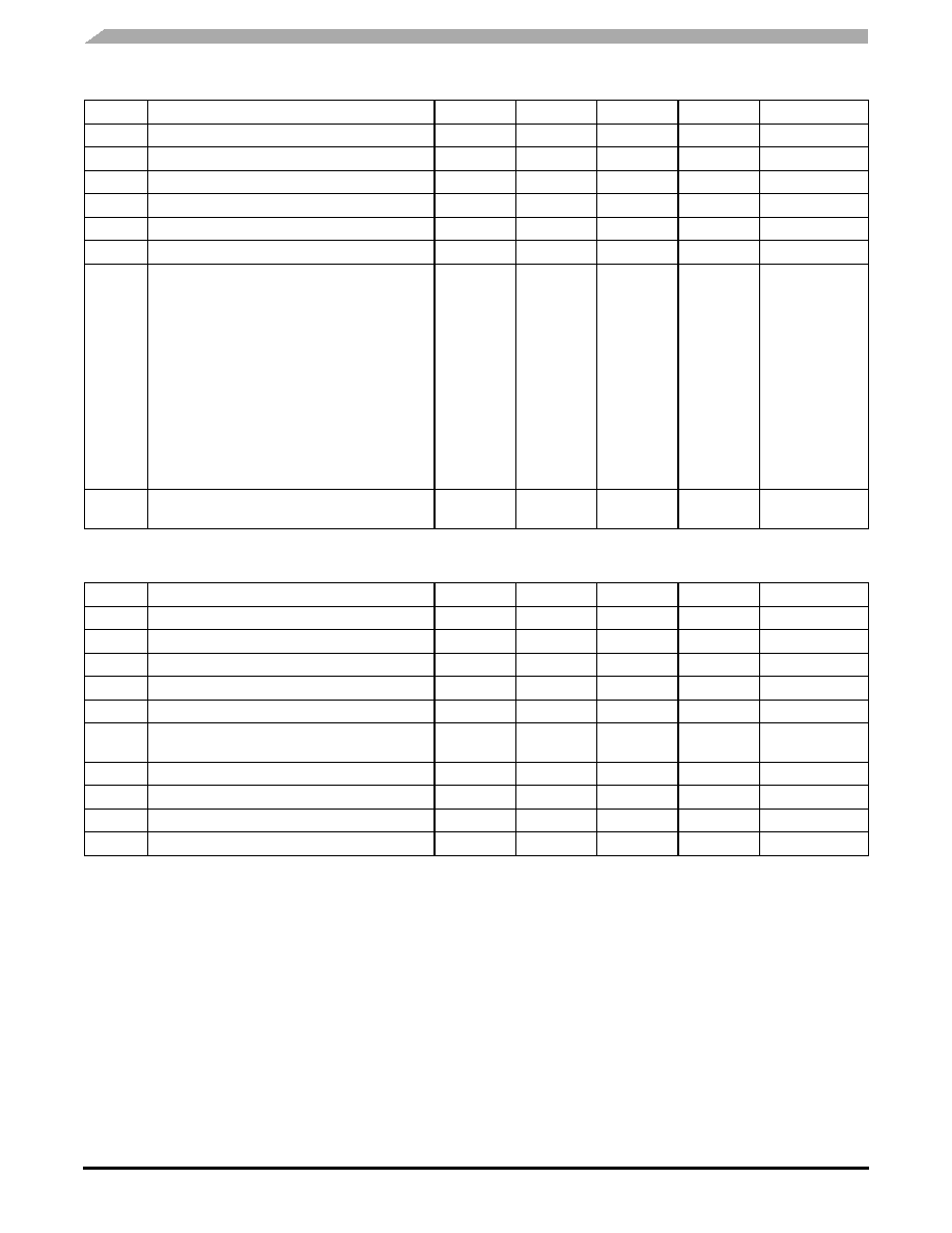
Table 4. General Specifications
Symbol
Characteristics
Min
Typ
Max
Unit
Condition
VTT
Output Termination Voltage
VCC ÷ 2
V
MM
ESD Protection (Machine Model)
200
V
HBM
ESD Protection (Human Body Model)
2000
V
LU
Latch-Up Immunity
200
mA
CPD
Power Dissipation Capacitance
10
pF
Per output
CIN
Input Capacitance
4.0
pF
Inputs
θJA
LQFP 32 Thermal resistance junction to ambient
JESD 51-3, single layer test board
JESD 51-6, 2S2P multilayer test board
83.1
73.3
68.9
63.8
57.4
59.0
54.4
52.5
50.4
47.8
86.0
75.4
70.9
65.3
59.6
60.6
55.7
53.8
51.5
48.8
°C/W
Natural
convection
100 ft/min
200 ft/min
400 ft/min
800 ft/min
Natural
convection
100 ft/min
200 ft/min
400 ft/min
800 ft/min
θJC
LQFP 32 Thermal resistance junction to case
23.0
26.3
°C/W
MIL-SPEC 883E
Method 1012.1
Table 5. DC Characteristics (VCC = 3.3 V ± 5%, TA = 0°C to 70°C)
Symbol
Characteristics
Min
Typ
Max
Unit
Condition
VIH
Input High Voltage
2.0
VCC + 0.3
V
LVCMOS
VIL
Input Low Voltage
0.8
V
LVCMOS
VPP
Peak-to-Peak Input Voltage
(PCLK)
250
mV
LVPECL
VCMR(1)
1. VCMR (DC) is the crosspoint of the differential input signal. Functional operation is obtained when the crosspoint is within the VCMR range
and the input swing lies within the VPP (DC) specification.
Common Mode Range
(PCLK)
1.0
VCC –0.6
V
LVPECL
VOH
Output High Voltage
2.4
V
IOH = –24 mA(2)
2. The MPC9658 is capable of driving 50
transmission lines on the incident edge. Each output drives one 50 parallel terminated
transmission line to a termination voltage of VTT. Alternatively, the device drives up to two 50 series terminated transmission lines.
VOL
Output Low Voltage(3)
3. The MPC9658 output levels are compatible to the MPC958 output levels.
0.55
0.30
V
IOL = 24 mA
IOL = 12 mA
ZOUT
Output Impedance
14 – 17
IIN
Input Current(4)
4. Inputs have pull-down resistors affecting the input current.
±200
A
VIN = VCC or GND
ICC_PLL Maximum PLL Supply Current
12
20
mA
VCC_PLL Pin
ICCQ
Maximum Quiescent Supply Current
13
20
mA
All VCC Pins
相关PDF资料 |
PDF描述 |
|---|---|
| MPC9658ACR2 | 9658 SERIES, PLL BASED CLOCK DRIVER, 10 TRUE OUTPUT(S), 0 INVERTED OUTPUT(S), PQFP32 |
| MPC973FA | 973 SERIES, PLL BASED CLOCK DRIVER, 12 TRUE OUTPUT(S), 0 INVERTED OUTPUT(S), PQFP52 |
| MPC974FAR2 | 974 SERIES, PLL BASED CLOCK DRIVER, 14 TRUE OUTPUT(S), 0 INVERTED OUTPUT(S), PQFP52 |
| MPC974FA | 974 SERIES, PLL BASED CLOCK DRIVER, 14 TRUE OUTPUT(S), 0 INVERTED OUTPUT(S), PQFP52 |
| MPC974FA | 974 SERIES, PLL BASED CLOCK DRIVER, 14 TRUE OUTPUT(S), 0 INVERTED OUTPUT(S), PQFP52 |
相关代理商/技术参数 |
参数描述 |
|---|---|
| MPC9658FAR2 | 制造商:Integrated Device Technology Inc 功能描述:PLL Clock Driver Single 32-Pin LQFP T/R 制造商:Integrated Device Technology Inc 功能描述:MPC9658FAR2 - Tape and Reel |
| MPC96877VK | 功能描述:时钟发生器及支持产品 DDR2 PLL RoHS:否 制造商:Silicon Labs 类型:Clock Generators 最大输入频率:14.318 MHz 最大输出频率:166 MHz 输出端数量:16 占空比 - 最大:55 % 工作电源电压:3.3 V 工作电源电流:1 mA 最大工作温度:+ 85 C 安装风格:SMD/SMT 封装 / 箱体:QFN-56 |
| MPC96877VKR2 | 功能描述:时钟发生器及支持产品 DDR2 PLL RoHS:否 制造商:Silicon Labs 类型:Clock Generators 最大输入频率:14.318 MHz 最大输出频率:166 MHz 输出端数量:16 占空比 - 最大:55 % 工作电源电压:3.3 V 工作电源电流:1 mA 最大工作温度:+ 85 C 安装风格:SMD/SMT 封装 / 箱体:QFN-56 |
| MPC970 | 制造商:MOTOROLA 制造商全称:Motorola, Inc 功能描述:LOW VOLTAGE PLL CLOCK DRIVER |
| MPC972 | 制造商:Motorola Inc 功能描述: |
发布紧急采购,3分钟左右您将得到回复。