- 您现在的位置:买卖IC网 > PDF目录2014 > MPC96877VK (IDT, Integrated Device Technology Inc)IC CLK DRIVER 1:10 SDRAM 52-BGA PDF资料下载
参数资料
| 型号: | MPC96877VK |
| 厂商: | IDT, Integrated Device Technology Inc |
| 文件页数: | 11/13页 |
| 文件大小: | 0K |
| 描述: | IC CLK DRIVER 1:10 SDRAM 52-BGA |
| 产品变化通告: | Product Discontinuation 09/Dec/2011 |
| 标准包装: | 1 |
| 类型: | 时钟缓冲器/驱动器,多路复用器 |
| PLL: | 是 |
| 主要目的: | 存储器,DDR2,SDRAM |
| 输入: | 时钟 |
| 输出: | SSTL-18 |
| 电路数: | 1 |
| 比率 - 输入:输出: | 1:10 |
| 差分 - 输入:输出: | 是/是 |
| 频率 - 最大: | 340MHz |
| 电源电压: | 1.7 V ~ 1.9 V |
| 工作温度: | 0°C ~ 70°C |
| 安装类型: | 表面贴装 |
| 封装/外壳: | 52-BGA |
| 包装: | 托盘 |
MPC96877
FREESCALE SEMICONDUCTOR ADVANCED CLOCK DRIVERS DEVICE DATA
553
NOTES:
1. There are two different terminations that are used with the following tests. The loadboard in Figure 2. IBIS Model Output Load is used to measure
the input and output differential-pair cross voltage only. The loadboard in Figure 3. Output Load Test Circuit 1 is used to measure all other tests.
For consistency, equal length cables must be used.
2. Static Phase offset does not include Jitter.
3. Period Jitter and Half-Period Jitter specifications are separate specifications that must be met independently of each other.
4. The Output Slew Rate is determined form the IBIS model into the load shown in Figure 4. Output Load Test Circuit 2. It is measured single ended.
5. To eliminate the impact of input slew rates on static phase offset, the input slew rates of Reference Clock Input CK, CK and Feedback Clock
Input FBIN, FBIN are recommended to be nearly equal. The 2.5 V/ns slew rates are shown as a recommended target. Compliance with these
Nom values is not mandatory if it can be adequately demonstrated that alternative characteristics meet the requirements of the registered DDR2
DIMM application.
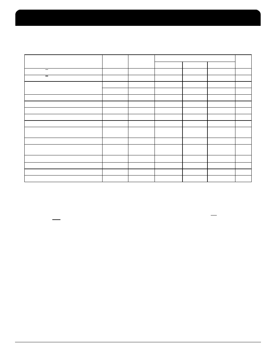
Table 7. Switching Characteristics over Recommended Free-Air Operating Temperature Range Unless Otherwise Noted
(see Notes)
Description
Parameter
Diagram
AVDD, VDDQ = 1.8 V ± 0.1 V
Unit
Min
Nom
Max
OE to any Y/Y
ten
see Figure 11
8
ns
OE to any Y/Y
tdis
see Figure 11
8
ns
Cycle-to-Cycle period jitter
tjit(cc+)
see Figure 4
0
40
ps
tjit(cc–)
0
–40
ps
Static phase offset
t(
)
see Figure 5
–50
50
ps
Dynamic phase offset
t(
)dyn
see Figure 10
–50
50
ps
Output clock skew
tsk(o)
see Figure 6
40
ps
Period Jitter
tjit(per)
see Figure 7
–40
40
ps
Half -period jitter
tjit(hper)
see Figure 8
–75
75
ps
Output Enable
slr(i)
see Figure 3
and Figure 9
0.5
V/ns
Input clock slew rate, measured single ended
1
2.5
4
Output clock slew rate, measured single ended
slr(o)
see Figure 3
and Figure 9
1.5
2.5
3
V/ns
Output differential-pair cross voltage
VOX
see Figure 2
(VDDQ/2) – 0.1
(VDDQ/2) + 0.1
V
SSC modulation frequency
30
33
kHz
SSC clock input frequency deviation
0.0
–0.5
PLL Loop bandwidth (–3dB from unity gain)
2.0
MHz
MPC96877
1.8 V PLL 1:10 Differential SDRAM Clock Driver
NETCOM
IDT 1.8 V PLL 1:10 Differential SDRAM Clock Driver
Freescale Timing Solutions Organization has been acquired by Integrated Device Technology, Inc
MPC96877
7
相关PDF资料 |
PDF描述 |
|---|---|
| MPC9773AE | IC PLL CLK GEN 1:12 3.3V 52-LQFP |
| MPC9850VF | IC PLL CLOCK GENERATOR 100MAPBGA |
| MPC9855VM | IC PLL CLOCK GENERATOR 100MAPBGA |
| MPC9893AE | IC PLL CLK GEN 1:12 3.3V 48-LQFP |
| MSTM-S3-TR-19.44M | IC MOD TIMING 19.440MHZ STRAT 3 |
相关代理商/技术参数 |
参数描述 |
|---|---|
| MPC96877VKR2 | 功能描述:时钟发生器及支持产品 DDR2 PLL RoHS:否 制造商:Silicon Labs 类型:Clock Generators 最大输入频率:14.318 MHz 最大输出频率:166 MHz 输出端数量:16 占空比 - 最大:55 % 工作电源电压:3.3 V 工作电源电流:1 mA 最大工作温度:+ 85 C 安装风格:SMD/SMT 封装 / 箱体:QFN-56 |
| MPC970 | 制造商:MOTOROLA 制造商全称:Motorola, Inc 功能描述:LOW VOLTAGE PLL CLOCK DRIVER |
| MPC972 | 制造商:Motorola Inc 功能描述: |
| MPC972FA | 制造商:Freescale Semiconductor 功能描述: |
| MPC972H10 F44A WAF | 制造商:Motorola Inc 功能描述: |
发布紧急采购,3分钟左右您将得到回复。