- 您现在的位置:买卖IC网 > PDF目录2014 > MPC9893AE (IDT, Integrated Device Technology Inc)IC PLL CLK GEN 1:12 3.3V 48-LQFP PDF资料下载
参数资料
| 型号: | MPC9893AE |
| 厂商: | IDT, Integrated Device Technology Inc |
| 文件页数: | 1/14页 |
| 文件大小: | 0K |
| 描述: | IC PLL CLK GEN 1:12 3.3V 48-LQFP |
| 标准包装: | 250 |
| 类型: | PLL 时钟发生器 |
| PLL: | 带旁路 |
| 输入: | LVCMOS |
| 输出: | LVCMOS |
| 电路数: | 1 |
| 比率 - 输入:输出: | 2:12 |
| 差分 - 输入:输出: | 无/无 |
| 频率 - 最大: | 200MHz |
| 除法器/乘法器: | 是/是 |
| 电源电压: | 2.375 V ~ 3.465 V |
| 工作温度: | -40°C ~ 85°C |
| 安装类型: | 表面贴装 |
| 封装/外壳: | 48-LQFP |
| 供应商设备封装: | 48-TQFP(7x7) |
| 包装: | 托盘 |
DATASHEET
3.3V 1:12 LVCMOS PLL Clock Generator
MPC9893
NRND
MPC9893 REVISION 8 JANUARY 16, 2013
1
2013 Integrated Device Technology, Inc.
The MPC9893 is a 2.5 V and 3.3 V compatible, PLL based intelligent dynamic
clock switch and generator specifically designed for redundant clock distribution
systems. The device receives two LVCMOS clock signals and generates 12
phase aligned output clocks. The MPC9893 is able to detect a failing reference
clock signal and to dynamically switch to a redundant clock signal. The switch
from the failing clock to the redundant clock occurs without interruption of the
output clock signal (output clock slews to alignment). The phase bump typically
caused by a clock failure is eliminated.
The device offers 12 low skew clock outputs organized into two output banks,
each configurable to support the different clock frequencies.
The extended temperature range of the MPC9893 supports
telecommunication and networking requirements. The device employs a fully
differential PLL design to minimize jitter.
Features
12-output LVCMOS PLL clock generator
2.5 V and 3.3 V compatible
IDCS - on-chip intelligent dynamic clock switch
Automatically detects clock failure
Smooth output phase transition during clock failover switch
7.5 – 200 MHz output frequency range
LVCMOS compatible inputs and outputs
External feedback enables zero-delay configurations
Supports networking, telecommunications and computer applications
Output enable/disable and static test mode (PLL bypass)
Low skew characteristics: maximum 50 ps output-to-output (within bank)
48-lead LQFP package, Pb-free
Ambient operating temperature range of -40 to 85
C
NRND – Not Recommend for New Designs
Functional Description
The MPC9893 is a 3.3 V or 2.5 V compatible PLL clock driver and clock generator. The clock generator uses a fully integrated
PLL to generate clock signals from redundant clock sources. The PLL multiplies the input reference clock signal by one, two,
three, four or eight. The frequency-multiplied clock drives six bank A outputs. Six bank B outputs can run at either the same fre-
quency than bank A or at half of the bank A frequency. Therefore, bank B outputs additionally support the frequency multiplication
of the input reference clock by 3
2 and 12. Bank A and bank B outputs are phase-aligned(1). Due to the external PLL feedback,
the clock signals of both output banks are also phase-aligned(1) to the selected input reference clock, providing virtually zero-de-
lay capability. The integrated IDCS continuously monitors both clock inputs and indicates a clock failure individually for each clock
input. When a false clock signal is detected, the MPC9893 switches to the redundant clock input, forcing the PLL to slowly slew
to alignment and not produce any phase bumps at the outputs. Both clock inputs are interchangeable, also supporting the switch
to a failed clock that was restored. The MPC9893 also provides a manual mode that allows for user-controlled clock switches.
The PLL bypass of the MPC9893 disables the IDCS and PLL-related specifications do not apply. In PLL bypass mode, the
MPC9893 is fully static in order to distribute low-frequency clocks for system test and diagnosis. Outputs of the MPC9893 can
be disabled (high-impedance tristate) to isolate the device from the system. Applying output disable also resets the MPC9893.
On power-up this reset function needs to be applied for correct operation of the circuitry. Please see the application section for
power-on sequence recommendations.
The device is packaged in a 7x7 mm2 48-lead LQFP package.
1. At coincident rising edges.
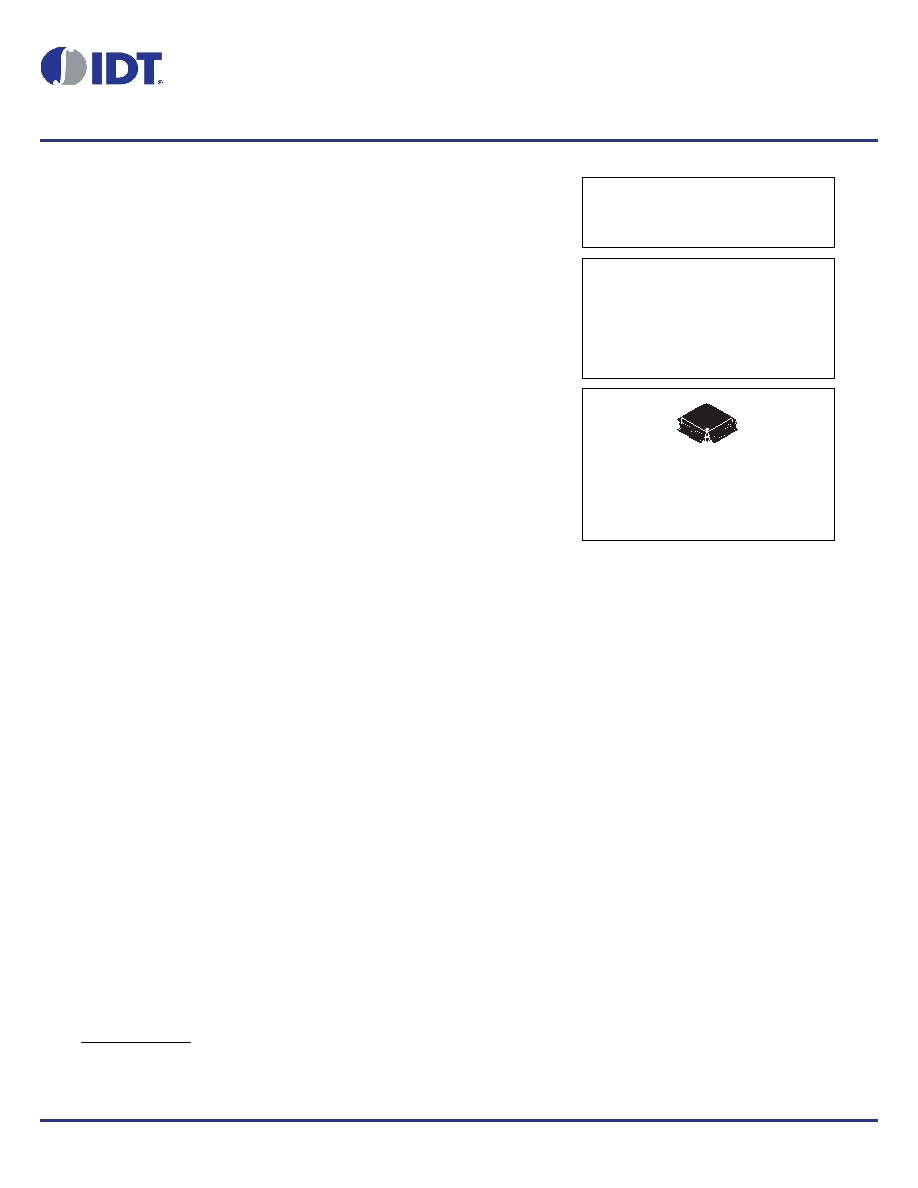
MPC9893
LOW VOLTAGE
2.5 V AND 3.3 V IDCS AND
PLL CLOCK GENERATOR
AE SUFFIX
48-LEAD LQFP PACKAGE
Pb-FREE PACKAGE
CASE 932-03
SCALE 2:1
NRND – Not Recommend for New Designs
相关PDF资料 |
PDF描述 |
|---|---|
| MSTM-S3-TR-19.44M | IC MOD TIMING 19.440MHZ STRAT 3 |
| MT5656RJ-92.R2 | MODEM SERIAL DATA V.92 5V |
| MT5656SMI-IP-92-SP | MODEM EMBEDDED SERIAL V.92 5V |
| MT9234SMI-P-HV-92-SP | MODEM V.92 PAR DATA V.34 FAX 5V |
| MX7224KCWN+ | IC DAC 8BIT CMOS PREC AMP 18SOIC |
相关代理商/技术参数 |
参数描述 |
|---|---|
| MPC9893AER2 | 功能描述:时钟发生器及支持产品 RoHS:否 制造商:Silicon Labs 类型:Clock Generators 最大输入频率:14.318 MHz 最大输出频率:166 MHz 输出端数量:16 占空比 - 最大:55 % 工作电源电压:3.3 V 工作电源电流:1 mA 最大工作温度:+ 85 C 安装风格:SMD/SMT 封装 / 箱体:QFN-56 |
| MPC9893FA | 功能描述:时钟发生器及支持产品 2.5 3.3V 200MHz Clock Generator RoHS:否 制造商:Silicon Labs 类型:Clock Generators 最大输入频率:14.318 MHz 最大输出频率:166 MHz 输出端数量:16 占空比 - 最大:55 % 工作电源电压:3.3 V 工作电源电流:1 mA 最大工作温度:+ 85 C 安装风格:SMD/SMT 封装 / 箱体:QFN-56 |
| MPC9893FAR2 | 制造商:Integrated Device Technology Inc 功能描述:PLL Clock Driver Single 48-Pin LQFP T/R 制造商:Integrated Device Technology Inc 功能描述:MPC9893FAR2 - Tape and Reel |
| MPC9894 | 制造商:未知厂家 制造商全称:未知厂家 功能描述:Quad Input Redundant IDCS Clock Generator |
| MPC9894VM | 制造商:IDT from Components Direct 功能描述:IDT MPC9894VM PLL - Trays 制造商:IDT 功能描述:IDT MPC9894VM PLL |
发布紧急采购,3分钟左右您将得到回复。