- 您现在的位置:买卖IC网 > PDF目录29137 > MPC97H74FAR2 (FREESCALE SEMICONDUCTOR INC) 97H SERIES, PLL BASED CLOCK DRIVER, 14 TRUE OUTPUT(S), 0 INVERTED OUTPUT(S), PQFP52 PDF资料下载
参数资料
| 型号: | MPC97H74FAR2 |
| 厂商: | FREESCALE SEMICONDUCTOR INC |
| 元件分类: | 时钟及定时 |
| 英文描述: | 97H SERIES, PLL BASED CLOCK DRIVER, 14 TRUE OUTPUT(S), 0 INVERTED OUTPUT(S), PQFP52 |
| 封装: | LQFP-52 |
| 文件页数: | 10/12页 |
| 文件大小: | 240K |
| 代理商: | MPC97H74FAR2 |
Advanced Clock Driver Devices
Freescale Semiconductor
7
MPC97H74
Using the MPC97H74 in Zero-Delay Applications
Nested clock trees are typical applications for the
MPC97H74. Designs using the MPC97H74 as LVCMOS PLL
fanout buffer with zero insertion delay will show significantly
lower clock skew than clock distributions developed from
CMOS fanout buffers. The external feedback of the
MPC97H74 clock driver allows for its use as a zero delay
buffer. The PLL aligns the feedback clock output edge with
the clock input reference edge resulting a near zero delay
through the device (the propagation delay through the device
is virtually eliminated). The maximum insertion delay of the
device in zero-delay applications is measured between the
reference clock input and any output. This effective delay
consists of the static phase offset, I/O jitter (phase or
long-term jitter), feedback path delay and the
output-to-output skew error relative to the feedback output.
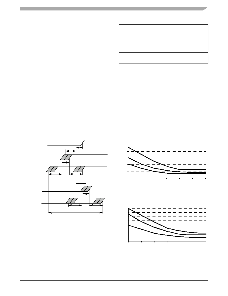
Calculation of Part-to-Part Skew
The MPC97H74 zero delay buffer supports applications
where critical clock signal timing can be maintained across
several devices. If the reference clock inputs of two or more
MPC97H74 are connected together, the maximum overall
timing uncertainty from the common CCLK input to any
output is:
tSK(PP) = t() + tSK(O) + tPD, LINE(FB) + tJIT() × CF
This maximum timing uncertainty consist of 4 components:
static phase offset, output skew, feedback board trace delay
and I/O (phase) jitter:
Due to the statistical nature of I/O jitter a rms value (1
σ) is
specified. I/O jitter numbers for other confidence factors (CF)
can be derived from Table 11.
The feedback trace delay is determined by the board
layout and can be used to fine-tune the effective delay
through each device.
Due to the frequency dependence of the static phase
offset and I/O jitter, using Figure 6. MPC97H74 I/O Jitter and
Figure 7. MPC97H74 I/O Jitter to predict a maximum I/O jitter
and the specified t() parameter relative to the input reference
frequency results in a precise timing performance analysis.
In the following example calculation a I/O jitter confidence
factor of 99.7 percent (
± 3 σ) is assumed, resulting in a worst
case timing uncertainty from the common input reference
clock to any output of –470 ps to +320 ps relative to CCLK
(PLL feedback =
÷8, reference frequency = 50 MHz, VCO
frequency = 400 MHz, I/O jitter = 15 ps rms max., static phase
offset t() = –250 ps to +100 ps):
tSK(PP) = [–250 ps...+100 ps] + [–175 ps...175 ps] +
[(15 ps
× –3)...(15 ps × 3)] + t
PD, LINE(FB)
tSK(PP) = [–470 ps...+320 ps] + tPD, LINE(FB)
Figure 5. MPC97H74 Max. Device-to-Device Skew
tPD, LINE(FB)
tJIT()
±tSK(O)
—t()
+t()
tJIT()
±tSK(O)
tSK(PP)
Max. Skew
CCLKCommon
QFBDevice 1
Any QDevice 1
QFBDevice2
Any QDevice 2
Table 11. Confidence Factor CF
CF
Probability of Clock Edge Within The Distribution
± 1σ
0.68268948
± 2σ
0.95449988
± 3σ
0.99730007
± 4σ
0.99993663
± 5σ
0.99999943
± 6σ
0.99999999
Maximum I/O Phase Jitter (RMS) versus Frequency
Parameter: PLL Feedback Divider FB
200
250
300
350
400
450
500
100
80
60
40
20
0
FB =
÷ 32
FB =
÷ 16
FB =
÷ 8
VCO Frequency (MHz)
t jit
(
)[p
s]
RMS
Figure 6. MPC97H74 I/O Jitter
Figure 7. MPC97H74 I/O Jitter
Maximum I/O Phase Jitter (RMS) versus Frequency
Parameter: PLL Feedback Divider FB
160
140
120
100
80
60
40
20
0
200
250
300
350
400
450
500
VCO Frequency (MHz)
t jit
(
)[ps]
RMS
FB
= ÷ 12
FB
= ÷ 48
FB
= ÷ 24
相关PDF资料 |
PDF描述 |
|---|---|
| MPC97H74FA | 97H SERIES, PLL BASED CLOCK DRIVER, 14 TRUE OUTPUT(S), 0 INVERTED OUTPUT(S), PQFP52 |
| MPC9893FAR2 | 9893 SERIES, PLL BASED CLOCK DRIVER, 12 TRUE OUTPUT(S), 0 INVERTED OUTPUT(S), PQFP48 |
| MPC991FAR2 | PLL BASED CLOCK DRIVER, 13 TRUE OUTPUT(S), 0 INVERTED OUTPUT(S), PQFP52 |
| MPC991FAR2 | PLL BASED CLOCK DRIVER, 13 TRUE OUTPUT(S), 0 INVERTED OUTPUT(S), PQFP52 |
| MPC993FA | 993 SERIES, PLL BASED CLOCK DRIVER, 5 TRUE OUTPUT(S), 0 INVERTED OUTPUT(S), PQFP32 |
相关代理商/技术参数 |
参数描述 |
|---|---|
| MPC980 | 制造商:MOTOROLA 制造商全称:Motorola, Inc 功能描述:DUAL 3.3V PLL CLOCK GENERATOR |
| MPC9817 | 制造商:FREESCALE 制造商全称:Freescale Semiconductor, Inc 功能描述:Clock Generator for PowerQUICC and PowerPC Microprocessors and Microcontrollers |
| MPC9817EN | 功能描述:时钟发生器及支持产品 FSL 1-5 PwrQUICC/Pwr PC Clk Gen, RoHS:否 制造商:Silicon Labs 类型:Clock Generators 最大输入频率:14.318 MHz 最大输出频率:166 MHz 输出端数量:16 占空比 - 最大:55 % 工作电源电压:3.3 V 工作电源电流:1 mA 最大工作温度:+ 85 C 安装风格:SMD/SMT 封装 / 箱体:QFN-56 |
| MPC9817ENR2 | 功能描述:时钟发生器及支持产品 FSL 1-5 PwrQUICC/Pwr PC Clk Gen, RoHS:否 制造商:Silicon Labs 类型:Clock Generators 最大输入频率:14.318 MHz 最大输出频率:166 MHz 输出端数量:16 占空比 - 最大:55 % 工作电源电压:3.3 V 工作电源电流:1 mA 最大工作温度:+ 85 C 安装风格:SMD/SMT 封装 / 箱体:QFN-56 |
| MPC9817SD | 功能描述:时钟发生器及支持产品 FSL 1-5 PwrQUICC/Pwr PC Clk Gen, RoHS:否 制造商:Silicon Labs 类型:Clock Generators 最大输入频率:14.318 MHz 最大输出频率:166 MHz 输出端数量:16 占空比 - 最大:55 % 工作电源电压:3.3 V 工作电源电流:1 mA 最大工作温度:+ 85 C 安装风格:SMD/SMT 封装 / 箱体:QFN-56 |
发布紧急采购,3分钟左右您将得到回复。