- 您现在的位置:买卖IC网 > PDF目录29137 > MPC97H74FAR2 (FREESCALE SEMICONDUCTOR INC) 97H SERIES, PLL BASED CLOCK DRIVER, 14 TRUE OUTPUT(S), 0 INVERTED OUTPUT(S), PQFP52 PDF资料下载
参数资料
| 型号: | MPC97H74FAR2 |
| 厂商: | FREESCALE SEMICONDUCTOR INC |
| 元件分类: | 时钟及定时 |
| 英文描述: | 97H SERIES, PLL BASED CLOCK DRIVER, 14 TRUE OUTPUT(S), 0 INVERTED OUTPUT(S), PQFP52 |
| 封装: | LQFP-52 |
| 文件页数: | 6/12页 |
| 文件大小: | 240K |
| 代理商: | MPC97H74FAR2 |
Advanced Clock Driver Devices
Freescale Semiconductor
3
MPC97H74
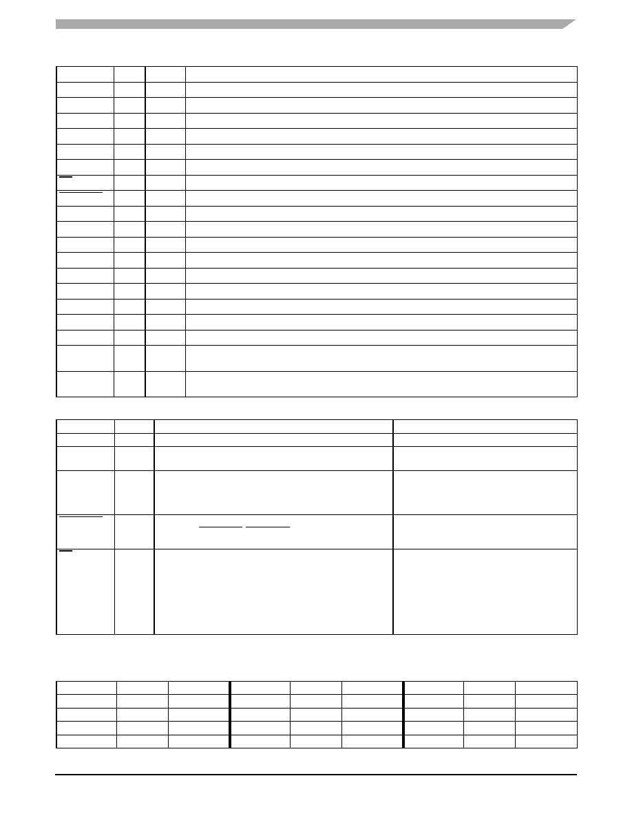
Table 1. Pin Configuration
Pin
I/O
Type
Function
CCLK0
Input
LVCMOS PLL reference clock
CCLK1
Input
LVCMOS Alternative PLL reference clock
FB_IN
Input
LVCMOS PLL feedback signal input, connect to QFB
CCLK_SEL
Input
LVCMOS LVCMOS clock reference select
VCO_SEL
Input
LVCMOS VCO operating frequency select
PLL_EN
Input
LVCMOS PLL enable/PLL bypass mode select
MR/OE
Input
LVCMOS Output enable/disable (high-impedance tristate) and device reset
CLK_STOP
Input
LVCMOS Output enable/clock stop (logic low state)
FSEL_A
Input
LVCMOS Frequency divider select for bank A outputs
FSEL_B
Input
LVCMOS Frequency divider select for bank B outputs
FSEL_C
Input
LVCMOS Frequency divider select for bank C outputs
FSEL_FB[1:0] Input
LVCMOS Frequency divider select for the QFB output
QA[4:0]
Output LVCMOS Clock outputs (bank A)
QB[4:0]
Output LVCMOS Clock outputs (bank B)
QC[3:0]
Output LVCMOS Clock outputs (bank C)
QFB
Output LVCMOS PLL feedback output. Connect to FB_IN.
GND
Supply Ground
Negative power supply
VCC_PLL
Supply VCC
PLL positive power supply (analog power supply). It is recommended to use an external RC filter for the
analog power supply pin VCC_PLL. Please see applications section for details.
VCC
Supply VCC
Positive power supply for I/O and core. All VCC pins must be connected to the positive power supply for
correct operation
Table 2. Function Table (MPC97H74 Configuration Controls)
Control
Default
0
1
CCLK_SEL
0
Selects CCLK0 as PLL reference signal input
Selects CCKL1 as PLL reference signal input
VCO_SEL
0
Selects VCO
÷ 2. The VCO frequency is scaled by a factor of 2
(high input frequency range)
Selects VCO
÷ 4. The VCO frequency is scaled
by a factor of 4 (low input frequency range).
PLL_EN
1
Test mode with the PLL bypassed. The reference clock is
substituted for the internal VCO output. MPC97H74 is fully static
and no minimum frequency limit applies. All PLL related AC
characteristics are not applicable.
Normal operation mode with PLL enabled.
CLK_STOP
1
QA, QB an QC outputs disabled in logic low state. QFB is not
affected by CLK_STOP. CLK_STOP deassertion may cause the
initial output clock pulse to be distorted.
Outputs enabled (active)
MR/OE
1
Outputs disabled (high-impedance state) and reset of the device.
During reset/output disable the PLL feedback loop is open and
the internal VCO is tied to its lowest frequency. The MPC97H74
requires reset after any loss of PLL lock. Loss of PLL lock may
occur when the external feedback path is interrupted. The length
of the reset pulse should be greater than one reference clock
cycle (CCLKx). The device is reset by the internal power-on reset
(POR) circuitry during power-up.
Outputs enabled (active)
VCO_SEL, FSEL_A, FSEL_B, FSEL_C and FSEL_FB[1:0] control the operating PLL frequency range and input/output frequency ratios.
Table 3. Function Table (Output Dividers Bank A, B, and C)
VCO_SEL
FSEL_A
QA[4:0]
VCO_SEL
FSEL_B
QB[4:0]
VCO_SEL
FSEL_C
QC[3:0]
0
VCO
÷ 4
0
VCO
÷ 4
0
VCO
÷ 8
0
1
VCO
÷ 8
0
1
VCO
÷ 8
0
1
VCO
÷ 12
1
0
VCO
÷ 8
1
0
VCO
÷ 8
1
0
VCO
÷ 16
1
VCO
÷ 16
1
VCO
÷ 16
1
VCO
÷ 24
相关PDF资料 |
PDF描述 |
|---|---|
| MPC97H74FA | 97H SERIES, PLL BASED CLOCK DRIVER, 14 TRUE OUTPUT(S), 0 INVERTED OUTPUT(S), PQFP52 |
| MPC9893FAR2 | 9893 SERIES, PLL BASED CLOCK DRIVER, 12 TRUE OUTPUT(S), 0 INVERTED OUTPUT(S), PQFP48 |
| MPC991FAR2 | PLL BASED CLOCK DRIVER, 13 TRUE OUTPUT(S), 0 INVERTED OUTPUT(S), PQFP52 |
| MPC991FAR2 | PLL BASED CLOCK DRIVER, 13 TRUE OUTPUT(S), 0 INVERTED OUTPUT(S), PQFP52 |
| MPC993FA | 993 SERIES, PLL BASED CLOCK DRIVER, 5 TRUE OUTPUT(S), 0 INVERTED OUTPUT(S), PQFP32 |
相关代理商/技术参数 |
参数描述 |
|---|---|
| MPC980 | 制造商:MOTOROLA 制造商全称:Motorola, Inc 功能描述:DUAL 3.3V PLL CLOCK GENERATOR |
| MPC9817 | 制造商:FREESCALE 制造商全称:Freescale Semiconductor, Inc 功能描述:Clock Generator for PowerQUICC and PowerPC Microprocessors and Microcontrollers |
| MPC9817EN | 功能描述:时钟发生器及支持产品 FSL 1-5 PwrQUICC/Pwr PC Clk Gen, RoHS:否 制造商:Silicon Labs 类型:Clock Generators 最大输入频率:14.318 MHz 最大输出频率:166 MHz 输出端数量:16 占空比 - 最大:55 % 工作电源电压:3.3 V 工作电源电流:1 mA 最大工作温度:+ 85 C 安装风格:SMD/SMT 封装 / 箱体:QFN-56 |
| MPC9817ENR2 | 功能描述:时钟发生器及支持产品 FSL 1-5 PwrQUICC/Pwr PC Clk Gen, RoHS:否 制造商:Silicon Labs 类型:Clock Generators 最大输入频率:14.318 MHz 最大输出频率:166 MHz 输出端数量:16 占空比 - 最大:55 % 工作电源电压:3.3 V 工作电源电流:1 mA 最大工作温度:+ 85 C 安装风格:SMD/SMT 封装 / 箱体:QFN-56 |
| MPC9817SD | 功能描述:时钟发生器及支持产品 FSL 1-5 PwrQUICC/Pwr PC Clk Gen, RoHS:否 制造商:Silicon Labs 类型:Clock Generators 最大输入频率:14.318 MHz 最大输出频率:166 MHz 输出端数量:16 占空比 - 最大:55 % 工作电源电压:3.3 V 工作电源电流:1 mA 最大工作温度:+ 85 C 安装风格:SMD/SMT 封装 / 箱体:QFN-56 |
发布紧急采购,3分钟左右您将得到回复。