- 您现在的位置:买卖IC网 > PDF目录9591 > MPC9850VMR2 (IDT, Integrated Device Technology Inc)IC PLL CLOCK GENERATOR 100MAPBGA PDF资料下载
参数资料
| 型号: | MPC9850VMR2 |
| 厂商: | IDT, Integrated Device Technology Inc |
| 文件页数: | 7/12页 |
| 文件大小: | 0K |
| 描述: | IC PLL CLOCK GENERATOR 100MAPBGA |
| 标准包装: | 1,000 |
| 类型: | 时钟/频率发生器,多路复用器 |
| PLL: | 是 |
| 主要目的: | 联网,PowerQUICC III,电信 |
| 输入: | LVCMOS,LVPECL,晶体 |
| 输出: | LVCMOS,LVDS |
| 电路数: | 1 |
| 比率 - 输入:输出: | 3:11 |
| 差分 - 输入:输出: | 是/是 |
| 频率 - 最大: | 500MHz |
| 电源电压: | 3.135 V ~ 3.465 V |
| 工作温度: | -40°C ~ 85°C |
| 安装类型: | 表面贴装 |
| 封装/外壳: | 100-LBGA |
| 供应商设备封装: | 100-CABGA(11x11) |
| 包装: | 带卷 (TR) |
MPC9850 Data Sheet
Clock Generator for PowerQUICC III
MPC9850 REVISION 6 FEBRUARY 6, 2013
4
2013 Integrated Device Technology, Inc.
OPERATION INFORMATION
Output Frequency Configuration
The MPC9850 was designed to provide the commonly
used frequencies in PowerQUICC, PowerPC and other
microprocessor systems. Table 3 lists the configuration
values that will generate those common frequencies. The
MPC9850 can generate numerous other frequencies that
may be useful in specific applications. The output frequency
(fout) of either Bank A or Bank B may be calculated by the
following equation.
fout = 2000 / N
where fout is in MHz and N = 2 * CLK_x[0:5]
This calculation is valid for all values of N from 8 to 126.
Note that N = 15 is a modified case of the configuration inputs
CLK_x[0:5]. To achieve N = 15 CLK_x[0:5] is configured to
00111 or 7.
Crystal Input Operation
TBD
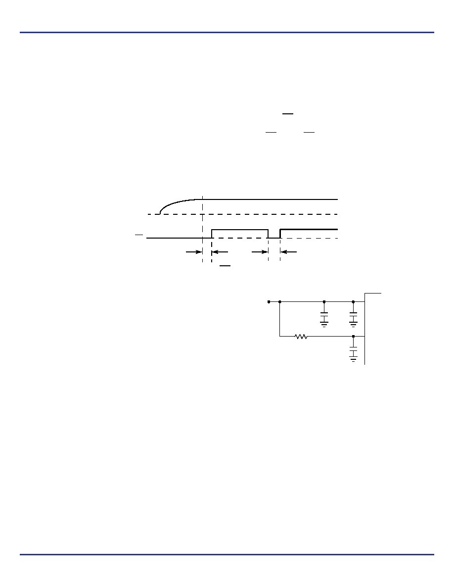
Power-Up and MR Operation
Figure 2 defines the release time and the minimum pulse
length for MR pin. The MR release time is based upon the
power supply being stable and within VDD specifications. See
Table 11 for actual parameter values. The MPC9850 may be
configured after release of reset and the outputs will be stable
for use after lock indication is obtained.
Figure 2. MR Operation
Power Supply Bypassing
The MPC9850 is a mixed analog/digital product. The
architecture of the MPC9850 supports low noise signal
operation at high frequencies. In order to maintain its superior
signal quality, all VDD pins should be bypassed by
high-frequency ceramic capacitors connected to GND. If the
spectral frequencies of the internally generated switching
noise on the supply pins cross the series resonant point of an
individual bypass capacitor, its overall impedance begins to
look inductive and thus increases with increasing frequency.
The parallel capacitor combination shown ensures that a low
impedance path to ground exists for frequencies well above
the noise bandwidth.
Figure 3. VCC Power Supply Bypass
MR
VDD
treset_rel
treset_pulse
VDD
MPC9850
0.1
F
22
F
0.1
F
15
VDD
VDDA
相关PDF资料 |
PDF描述 |
|---|---|
| CY2SSTV857ZXC-32T | IC CLK DDR266/333BUF1:10 48TSSOP |
| ICS9DB202CFLFT | IC JITTER ATTENUATOR 20-SSOP |
| MS3128F16-26P | CONN RCPT 26POS WALL MNT W/PINS |
| MS3128F14-12S | CONN RCPT 12POS WALL MNT W/SCKT |
| SL28504BZI-2T | IC CLOCK GEN EAGLELAKE 56TSSOP |
相关代理商/技术参数 |
参数描述 |
|---|---|
| MPC9855 | 制造商:MOTOROLA 制造商全称:Motorola, Inc 功能描述:Clock Generator for PowerQUICC and PowerPC Microprocessors |
| MPC9855VM | 功能描述:时钟发生器及支持产品 RoHS:否 制造商:Silicon Labs 类型:Clock Generators 最大输入频率:14.318 MHz 最大输出频率:166 MHz 输出端数量:16 占空比 - 最大:55 % 工作电源电压:3.3 V 工作电源电流:1 mA 最大工作温度:+ 85 C 安装风格:SMD/SMT 封装 / 箱体:QFN-56 |
| MPC9855VMR2 | 功能描述:时钟发生器及支持产品 RoHS:否 制造商:Silicon Labs 类型:Clock Generators 最大输入频率:14.318 MHz 最大输出频率:166 MHz 输出端数量:16 占空比 - 最大:55 % 工作电源电压:3.3 V 工作电源电流:1 mA 最大工作温度:+ 85 C 安装风格:SMD/SMT 封装 / 箱体:QFN-56 |
| MPC9865VM | 功能描述:时钟发生器及支持产品 RoHS:否 制造商:Silicon Labs 类型:Clock Generators 最大输入频率:14.318 MHz 最大输出频率:166 MHz 输出端数量:16 占空比 - 最大:55 % 工作电源电压:3.3 V 工作电源电流:1 mA 最大工作温度:+ 85 C 安装风格:SMD/SMT 封装 / 箱体:QFN-56 |
| MPC9865VMR2 | 功能描述:时钟发生器及支持产品 RoHS:否 制造商:Silicon Labs 类型:Clock Generators 最大输入频率:14.318 MHz 最大输出频率:166 MHz 输出端数量:16 占空比 - 最大:55 % 工作电源电压:3.3 V 工作电源电流:1 mA 最大工作温度:+ 85 C 安装风格:SMD/SMT 封装 / 箱体:QFN-56 |
发布紧急采购,3分钟左右您将得到回复。