- 您现在的位置:买卖IC网 > PDF目录8989 > MPC9893AER2 (IDT, Integrated Device Technology Inc)IC PLL CLK GEN 1:12 3.3V 48-LQFP PDF资料下载
参数资料
| 型号: | MPC9893AER2 |
| 厂商: | IDT, Integrated Device Technology Inc |
| 文件页数: | 13/14页 |
| 文件大小: | 0K |
| 描述: | IC PLL CLK GEN 1:12 3.3V 48-LQFP |
| 标准包装: | 2,000 |
| 类型: | PLL 时钟发生器 |
| PLL: | 带旁路 |
| 输入: | LVCMOS |
| 输出: | LVCMOS |
| 电路数: | 1 |
| 比率 - 输入:输出: | 2:12 |
| 差分 - 输入:输出: | 无/无 |
| 频率 - 最大: | 200MHz |
| 除法器/乘法器: | 是/是 |
| 电源电压: | 2.375 V ~ 3.465 V |
| 工作温度: | -40°C ~ 85°C |
| 安装类型: | 表面贴装 |
| 封装/外壳: | 48-LQFP |
| 供应商设备封装: | 48-TQFP(7x7) |
| 包装: | 带卷 (TR) |
MPC9893 REVISION 8 JANUARY 16, 2013
8
2013 Integrated Device Technology, Inc.
MPC9893 Data Sheet
3.3V 1:12 LVCMOS PLL CLOCK GENERATOR
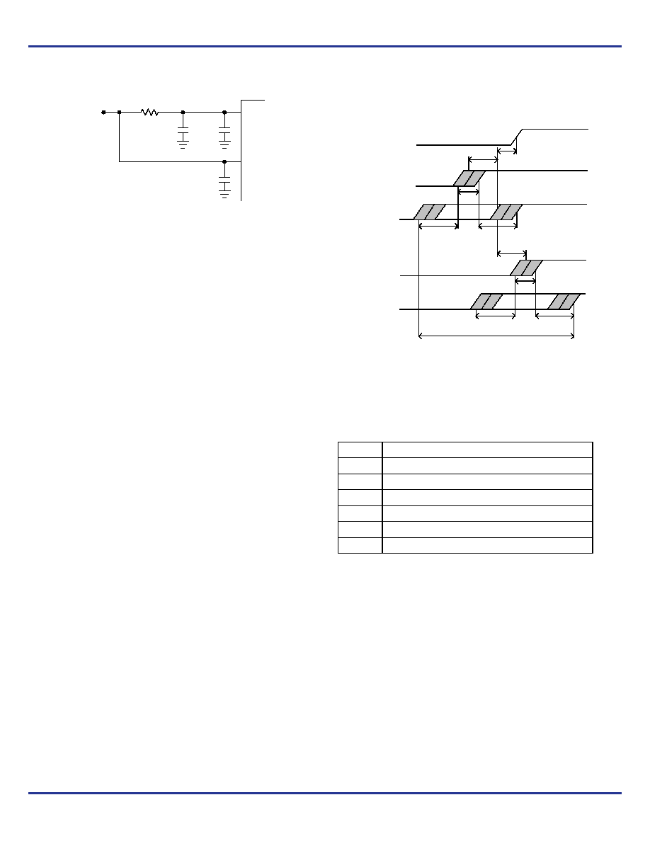
Figure 3. VCC_PLL Power Supply Filter
The minimum values for RF and the filter capacitor CF are
defined by the required filter characteristics: the RC filter
should provide an attenuation greater than 40 dB for noise
whose spectral content is above 100 kHz. In the example RC
filter shown in Figure 3, the filter cut-off frequency is around
3-5 kHz and the noise attenuation at 100 kHz is better than
42 dB.
As the noise frequency crosses the series resonant point
of an individual capacitor its overall impedance begins to look
inductive and thus increases with increasing frequency. The
parallel capacitor combination shown ensures that a low
impedance path to ground exists for frequencies well above
the bandwidth of the PLL. Although the MPC9893 has
several design features to minimize the susceptibility to
power supply noise (isolated power and grounds and fully
differential PLL) there still may be applications in which
overall performance is being degraded due to system power
supply noise. The power supply filter schemes discussed in
this section should be adequate to eliminate power supply
noise related problems in most designs.
Using the MPC9893 in Zero-Delay Applications
Nested clock trees are typical applications for the
MPC9893. Designs using the MPC9893 as LVCMOS PLL
fanout buffer with zero insertion delay will show significantly
lower clock skew than clock distributions developed from
CMOS fanout buffers. The external feedback option of the
MPC9893 clock driver allows for its use as a zero delay
buffer. The the propagation delay through the device is
virtually eliminated. The PLL aligns the feedback clock output
edge with the clock input reference edge resulting a near zero
delay through the device. The maximum insertion delay of the
device in zero-delay applications is measured between the
reference clock input and any output. This effective delay
consists of the static phase offset, I/O jitter (phase or long-
term jitter), feedback path delay and the output-to-output
skew error relative to the feedback output.
Calculation of Part-to-Part Skew
The MPC9893 zero delay buffer supports applications
where critical clock signal timing can be maintained across
several devices. If the reference clock inputs of two or more
MPC9893 are connected together, the maximum overall
timing uncertainty from the common CLK0 or CLK1 input to
any output is:
tSK(PP) = t() + tSK(O) + tPD, LINE(FB) + tJIT() CF
This maximum timing uncertainty consist of four
components: static phase offset, output skew, feedback
board trace delay and I/O (phase) jitter:
Figure 4. MPC9893 Max. Device-to-Device Skew
Due to the statistical nature of I/O jitter a RMS value (1
)
is specified. I/O jitter numbers for other confidence factors
(CF) can be derived from Table 9.
The feedback trace delay is determined by the board
layout and can be used to fine-tune the effective delay
through each device. In the following example calculation a I/
O jitter confidence factor of 99.7% (
3) is assumed,
resulting in a worst case timing uncertainty from the common
clock input to any MPC9893 output of –275 ps to +265 ps
relative to the reference clock input CLK0/1:
tSK(PP) = [–60ps...50ps] + [-125ps...125ps] +
[(30ps
–3)...(30ps 3)] + tPD, LINE(FB)
tSK(PP) = [–275ps...265ps] + tPD, LINE(FB)
Example configuration:
fref = 100 MHz, VCC = 3.3 V
fVCO = 400 MHz, FSEL[0:2]=111
VCC_PLL
VCC
MPC9893
10 nF
RF = 5–15
CF = 22F
CF
33...100 nF
RF
VCC
Table 9. Confidence Factor CF
CF
Probability of clock edge within the distribution
1
0.68268948
2
0.95449988
3
0.99730007
4
0.99993663
5
0.99999943
6
0.99999999
tPD,LINE(FB)
tJIT()
+tSK(O)
—t()
+t()
tJIT()
+tSK(O)
tSK(PP)
Max. skew
TCLKCommon
QFBDevice 1
Any QDevice 1
QFBDevice2
Any QDevice 2
相关PDF资料 |
PDF描述 |
|---|---|
| VE-JTM-MZ-F4 | CONVERTER MOD DC/DC 10V 25W |
| VI-BN3-MV-F1 | CONVERTER MOD DC/DC 24V 150W |
| VI-BNJ-MV-F4 | CONVERTER MOD DC/DC 36V 150W |
| VI-BNJ-MV-F3 | CONVERTER MOD DC/DC 36V 150W |
| LTC1452IS8#PBF | IC D/A CONV 12BIT R-R 8-SOIC |
相关代理商/技术参数 |
参数描述 |
|---|---|
| MPC9893FA | 功能描述:时钟发生器及支持产品 2.5 3.3V 200MHz Clock Generator RoHS:否 制造商:Silicon Labs 类型:Clock Generators 最大输入频率:14.318 MHz 最大输出频率:166 MHz 输出端数量:16 占空比 - 最大:55 % 工作电源电压:3.3 V 工作电源电流:1 mA 最大工作温度:+ 85 C 安装风格:SMD/SMT 封装 / 箱体:QFN-56 |
| MPC9893FAR2 | 制造商:Integrated Device Technology Inc 功能描述:PLL Clock Driver Single 48-Pin LQFP T/R 制造商:Integrated Device Technology Inc 功能描述:MPC9893FAR2 - Tape and Reel |
| MPC9894 | 制造商:未知厂家 制造商全称:未知厂家 功能描述:Quad Input Redundant IDCS Clock Generator |
| MPC9894VM | 制造商:IDT from Components Direct 功能描述:IDT MPC9894VM PLL - Trays 制造商:IDT 功能描述:IDT MPC9894VM PLL |
| MPC990 | 制造商:MOTOROLA 制造商全称:Motorola, Inc 功能描述:LOW VOLTAGE PLL CLOCK DRIVER |
发布紧急采购,3分钟左右您将得到回复。