- 您现在的位置:买卖IC网 > PDF目录8989 > MPC9893AER2 (IDT, Integrated Device Technology Inc)IC PLL CLK GEN 1:12 3.3V 48-LQFP PDF资料下载
参数资料
| 型号: | MPC9893AER2 |
| 厂商: | IDT, Integrated Device Technology Inc |
| 文件页数: | 14/14页 |
| 文件大小: | 0K |
| 描述: | IC PLL CLK GEN 1:12 3.3V 48-LQFP |
| 标准包装: | 2,000 |
| 类型: | PLL 时钟发生器 |
| PLL: | 带旁路 |
| 输入: | LVCMOS |
| 输出: | LVCMOS |
| 电路数: | 1 |
| 比率 - 输入:输出: | 2:12 |
| 差分 - 输入:输出: | 无/无 |
| 频率 - 最大: | 200MHz |
| 除法器/乘法器: | 是/是 |
| 电源电压: | 2.375 V ~ 3.465 V |
| 工作温度: | -40°C ~ 85°C |
| 安装类型: | 表面贴装 |
| 封装/外壳: | 48-LQFP |
| 供应商设备封装: | 48-TQFP(7x7) |
| 包装: | 带卷 (TR) |
MPC9893 REVISION 8 JANUARY 16, 2013
9
2013 Integrated Device Technology, Inc.
MPC9893 Data Sheet
3.3V 1:12 LVCMOS PLL CLOCK GENERATOR
The I/O (Phase) jitter of the MPC9893 depends on the
internal VCO frequency and the PLL feedback divider
configuration. A high internal VCO frequency and a low PLL
feedback divider result in lower I/O jitter than the jitter limits in
the AC characteristics (Table 8). When calculating the part-
to-part skew, Table 10 should be used to determine the actual
VCO frequency, then use Figure 5 to determine the maximum
I/O jitter for the specific VCO frequency and divider
configuration. In above example calculation, the internal VCO
frequency of 400 MHz corresponds to a maximum I/O jitter of
30 ps (RMS).
Figure 5. Max. I/O Phase Jitter versus VCO Frequency
The cycle-to-cycle jitter and period jitter of the MPC9893
depend on the output configuration and on the frequency of
the internal VCO. Using the outputs of bank A and bank B at
the same frequency (FSEL3=0) results in a lower jitter than
the split output frequency configuration (FSEL3=1). The jitter
also decreases with an increasing internal VCO frequency.
MPC9893.
Figure 6. Max. Cycle-to-Cycle Jitter versus
VCO Frequency
Figure 7. Max. Period Jitter versus VCO Frequency
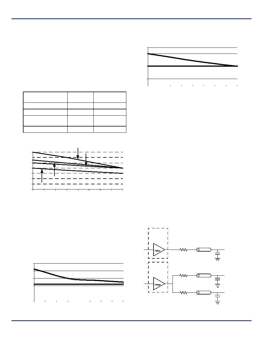
Driving Transmission Lines
The MPC9893 clock driver was designed to drive high
speed signals in a terminated transmission line environment.
To provide the optimum flexibility to the user the output
drivers were designed to exhibit the lowest impedance
possible. With an output impedance of less than 20
the
drivers can drive either parallel or series terminated
transmission lines. For more information on transmission
lines the reader is referred to Freescale Semiconductor
application note AN1091. In most high performance clock
networks point-to-point distribution of signals is the method of
choice. In a point-to-point scheme either series terminated or
parallel terminated transmission lines can be used. The
parallel technique terminates the signal at the end of the line
with a 50
resistance to VCC2.
This technique draws a fairly high level of DC current and
thus only a single terminated line can be driven by each
output of the MPC9893 clock driver. For the series terminated
case however there is no DC current draw, thus the outputs
can drive multiple series terminated lines. Figure 8 illustrates
an output driving a single series terminated line versus two
series terminated lines in parallel. When taken to its extreme
the fanout of the MPC9893 clock driver is effectively doubled
due to its capability to drive multiple lines.
Figure 8. Single versus Dual Transmission Lines
Table 10. Internal VCO Frequency fVCO
MPC9893
Configuration
fVCO
PLL Feedback
Divider FB
M1H, M12H, M2H, M22H
4 * fref
4
M3, M32
6 * fref
6
M1M, M12M, M2M, M22M,
M4, M42
8 * fref
8
M1L, M12L, M8, M82
16 * fref
16
I/O Phase Jitter versus Frequency
Parameter: PLL/Feedback Configuration
FB=16: FSEL[0:2]=000, 101
FB=8: FSEL[0:2]=001, 011, 110
FB=6: FSEL[0:2}=010
FB=4: FSEL[0:2]=100, 111
70
60
50
40
30
20
10
0
t jit
(
)[p
s]
RMS
240
260
280
300
320
340
360
380
400
VCO frequency [MHz]
Cycle-to-Cycle Jitter versus Frequency
Parameter: Output Configuration
500
400
300
200
100
0
240
260
280
300
320
340
360
380
400
VCO frequency [MHz]
t jit
(cc
)[p
s]
PSEL3=1
PSEL3=0
Period Jitter versus Frequency
Parameter: Output Configuration
PSEL=xxx1
PSEL=xxx0
300
250
200
150
100
50
0
240
260
280
300
320
340
360
380
400
VCO frequency [MHz]
t jit(
pe
r)[ps
]
14
In
MPC9893
Output
Buffer
RS = 36
ZO = 50
OutA
14
In
MPC9893
Output
Buffer
RS = 36
ZO = 50
OutB0
RS = 36
ZO = 50
OutB1
相关PDF资料 |
PDF描述 |
|---|---|
| VE-JTM-MZ-F4 | CONVERTER MOD DC/DC 10V 25W |
| VI-BN3-MV-F1 | CONVERTER MOD DC/DC 24V 150W |
| VI-BNJ-MV-F4 | CONVERTER MOD DC/DC 36V 150W |
| VI-BNJ-MV-F3 | CONVERTER MOD DC/DC 36V 150W |
| LTC1452IS8#PBF | IC D/A CONV 12BIT R-R 8-SOIC |
相关代理商/技术参数 |
参数描述 |
|---|---|
| MPC9893FA | 功能描述:时钟发生器及支持产品 2.5 3.3V 200MHz Clock Generator RoHS:否 制造商:Silicon Labs 类型:Clock Generators 最大输入频率:14.318 MHz 最大输出频率:166 MHz 输出端数量:16 占空比 - 最大:55 % 工作电源电压:3.3 V 工作电源电流:1 mA 最大工作温度:+ 85 C 安装风格:SMD/SMT 封装 / 箱体:QFN-56 |
| MPC9893FAR2 | 制造商:Integrated Device Technology Inc 功能描述:PLL Clock Driver Single 48-Pin LQFP T/R 制造商:Integrated Device Technology Inc 功能描述:MPC9893FAR2 - Tape and Reel |
| MPC9894 | 制造商:未知厂家 制造商全称:未知厂家 功能描述:Quad Input Redundant IDCS Clock Generator |
| MPC9894VM | 制造商:IDT from Components Direct 功能描述:IDT MPC9894VM PLL - Trays 制造商:IDT 功能描述:IDT MPC9894VM PLL |
| MPC990 | 制造商:MOTOROLA 制造商全称:Motorola, Inc 功能描述:LOW VOLTAGE PLL CLOCK DRIVER |
发布紧急采购,3分钟左右您将得到回复。