- 您现在的位置:买卖IC网 > PDF目录8989 > MPC9893AER2 (IDT, Integrated Device Technology Inc)IC PLL CLK GEN 1:12 3.3V 48-LQFP PDF资料下载
参数资料
| 型号: | MPC9893AER2 |
| 厂商: | IDT, Integrated Device Technology Inc |
| 文件页数: | 8/14页 |
| 文件大小: | 0K |
| 描述: | IC PLL CLK GEN 1:12 3.3V 48-LQFP |
| 标准包装: | 2,000 |
| 类型: | PLL 时钟发生器 |
| PLL: | 带旁路 |
| 输入: | LVCMOS |
| 输出: | LVCMOS |
| 电路数: | 1 |
| 比率 - 输入:输出: | 2:12 |
| 差分 - 输入:输出: | 无/无 |
| 频率 - 最大: | 200MHz |
| 除法器/乘法器: | 是/是 |
| 电源电压: | 2.375 V ~ 3.465 V |
| 工作温度: | -40°C ~ 85°C |
| 安装类型: | 表面贴装 |
| 封装/外壳: | 48-LQFP |
| 供应商设备封装: | 48-TQFP(7x7) |
| 包装: | 带卷 (TR) |
MPC9893 REVISION 8 JANUARY 16, 2013
3
2013 Integrated Device Technology, Inc.
MPC9893 Data Sheet
3.3V 1:12 LVCMOS PLL CLOCK GENERATOR
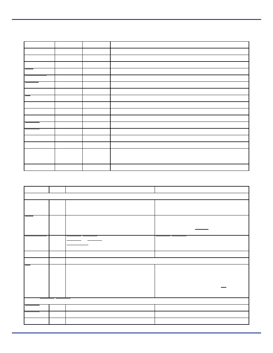
Table 1. Pin Configurations
Number
Name
Type
Description
CLK0, CLK1
Input
LVCMOS
PLL reference clock inputs
FB
Input
LVCMOS
PLL feedback signal input, connect directly to QFB output
REF_SEL
Input
LVCMOS
Selects the primary reference clock
MAN/A
Input
LVCMOS
Selects automatic switch mode or manual reference clock selection
ALARM_RST
Input
LVCMOS
Reset of alarm flags and selected reference clock
PLL_EN
Input
LVCMOS
Select PLL or static test mode
FSEL[0:3]
Input
LVCMOS
Clock frequency selection and configuration of clock divider modes
OE/MR
Input
LVCMOS
Output enable/disable and device reset
QA[0:5]
Output
LVCMOS
Bank A clock outputs
QB[0:5]
Output
LVCMOS
Bank B clock outputs
QFB
Output
LVCMOS
Clock feedback output. QFB must be connected to FB for correct operation
ALARM0
Output
LVCMOS
Indicates clock failure on CLK0
ALARM1
Output
LVCMOS
Indicates clock failure on CLK1
CLK_IND
Output
LVCMOS
Indicates currently selected input reference clock
GND
Supply
Ground
Negative power supply
VCC_PLL
Supply
VCC
Positive power supply for the PLL (analog power supply). It is recommended to use an
external RC filter for the analog power supply pin VCC_PLL. Please see the application
section for details.
VCC
Supply
VCC
Positive power supply for I/O and core
Table 2. Function Table
Control
Default
0
1
Inputs
PLL_EN
0
PLL enabled. The input to output frequency relationship
is that according to Table 3 if the PLL is frequency
locked.
PLL bypassed and IDCS disabled. The VCO output is
replaced by the reference clock signal fref. The MPC9893
is in manual mode.
MAN/A
1
Manual clock switch mode. IDCS disabled. Clock
failure detection and output flags ALARM0, ALARM1,
CLK_IND are enabled.
Automatic clock switch mode. IDCS enabled. Clock failure
detection and output flags ALARM0, ALARM1, CLK_IND
are enabled. IDCS overrides REF_SEL on a clock failure.
IDCS operation requires PLL_EN = 0.
ALARM_RST
1
ALARM0, ALARM1 and CLK_IND flags are reset:
ALARM0=H, ALARM1=H and CLK_IND=REF_SEL.
ALARM_RST is a one-shot function.
ALARM0, ALARM1 and CLK_IND active
REF_SEL
0
Selects CLK0 as the primary clock source
Selects CLK1 as the secondary clock source
FSEL[0:3]
0000
See Table 3
OE/MR
0
Outputs enabled (active)
Outputs disabled (high impedance tristate), reset of data
generators and output dividers. The MPC9893 requires
reset at power-up and after any loss of PLL lock. Loss of
PLL lock may occur when the external feedback path is
interrupted. The length of the reset pulse should be greater
than two reference clock cycles (CLK0,1). OE/MR does not
tristate the QFB output.
Outputs (ALARM0, ALARM1, CLK_IND are valid if PLL is locked)
ALARM0
CLK0 failure
ALARM1
CLK1 failure
CLK_IND
CLK0 is the reference clock
CLK1 is the reference clock
相关PDF资料 |
PDF描述 |
|---|---|
| VE-JTM-MZ-F4 | CONVERTER MOD DC/DC 10V 25W |
| VI-BN3-MV-F1 | CONVERTER MOD DC/DC 24V 150W |
| VI-BNJ-MV-F4 | CONVERTER MOD DC/DC 36V 150W |
| VI-BNJ-MV-F3 | CONVERTER MOD DC/DC 36V 150W |
| LTC1452IS8#PBF | IC D/A CONV 12BIT R-R 8-SOIC |
相关代理商/技术参数 |
参数描述 |
|---|---|
| MPC9893FA | 功能描述:时钟发生器及支持产品 2.5 3.3V 200MHz Clock Generator RoHS:否 制造商:Silicon Labs 类型:Clock Generators 最大输入频率:14.318 MHz 最大输出频率:166 MHz 输出端数量:16 占空比 - 最大:55 % 工作电源电压:3.3 V 工作电源电流:1 mA 最大工作温度:+ 85 C 安装风格:SMD/SMT 封装 / 箱体:QFN-56 |
| MPC9893FAR2 | 制造商:Integrated Device Technology Inc 功能描述:PLL Clock Driver Single 48-Pin LQFP T/R 制造商:Integrated Device Technology Inc 功能描述:MPC9893FAR2 - Tape and Reel |
| MPC9894 | 制造商:未知厂家 制造商全称:未知厂家 功能描述:Quad Input Redundant IDCS Clock Generator |
| MPC9894VM | 制造商:IDT from Components Direct 功能描述:IDT MPC9894VM PLL - Trays 制造商:IDT 功能描述:IDT MPC9894VM PLL |
| MPC990 | 制造商:MOTOROLA 制造商全称:Motorola, Inc 功能描述:LOW VOLTAGE PLL CLOCK DRIVER |
发布紧急采购,3分钟左右您将得到回复。