- 您现在的位置:买卖IC网 > PDF目录29137 > MPC9952FA (MOTOROLA INC) PLL BASED CLOCK DRIVER, 11 TRUE OUTPUT(S), 0 INVERTED OUTPUT(S), PQFP32 PDF资料下载
参数资料
| 型号: | MPC9952FA |
| 厂商: | MOTOROLA INC |
| 元件分类: | 时钟及定时 |
| 英文描述: | PLL BASED CLOCK DRIVER, 11 TRUE OUTPUT(S), 0 INVERTED OUTPUT(S), PQFP32 |
| 封装: | PLASTIC, LQFP-32 |
| 文件页数: | 3/5页 |
| 文件大小: | 96K |
| 代理商: | MPC9952FA |
MPC9952
MOTOROLA ADVANCED CLOCK DRIVERS DEVICE DATA
284
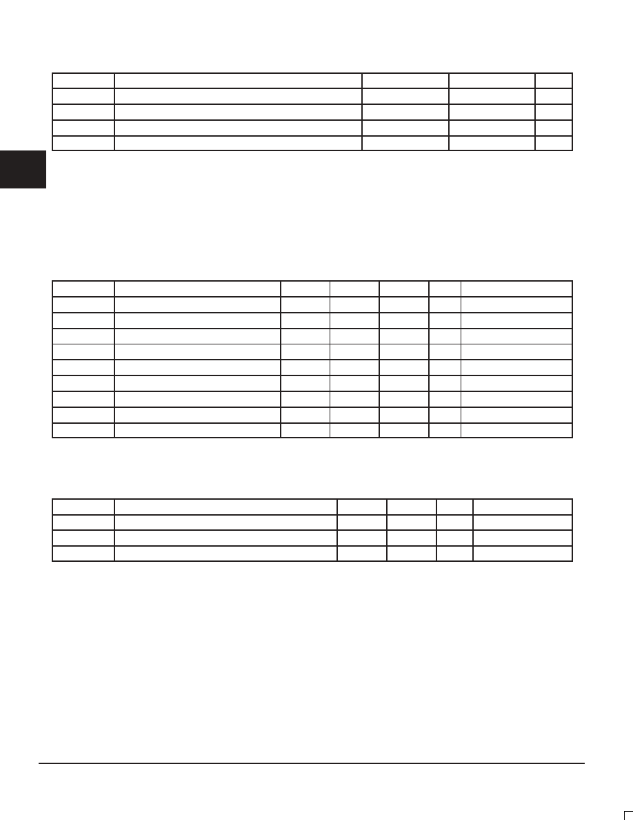
ABSOLUTE MAXIMUM RATINGS*
Symbol
Parameter
Min
Max
Unit
VCC
Supply Voltage
–0.3
4.6
V
VI
Input Voltage
–0.3
VCC + 0.3
V
IIN
Input Current
±20
mA
TStor
Storage Temperature Range
–40
125
°C
* Absolute maximum continuous ratings are those values beyond which damage to the device may occur. Exposure to these conditions or condi-
tions beyond those indicated may adversely affect device reliability. Functional operation under absolute-maximum-rated conditions is not im-
plied.
THERMAL CHARACTERISTICS
Proper thermal management is critical for reliable system operation. This is especially true for high fanout and high drive capa-
bility products. Generic thermal information is available for the Motorola Clock Driver products. The means of calculating die
power, the corresponding die temperature and the relationship to longterm reliability is addressed in the Motorola application
note AN1545.
DC CHARACTERISTICS (TA = 0° to 70°C, VCCO = VCCI = VCCA = 3.3V ± 5%)
Symbol
Characteristic
Min
Typ
Max
Unit
Condition
VIH
Input HIGH Voltage
2.0
3.6
V
VIL
Input LOW Voltage
0.8
V
VOH
Output HIGH Voltage
2.4
V
IOH = –20mA (Note 1.)
VOL
Output LOW Voltage
0.5
V
IOL = 20mA (Note 1.)
IIN
Input Current
±120
A
Note 2.
CIN
Input Capacitance
2.7
4.0
pF
Cpd
Power Dissipation Capacitance
25
pF
ICC
Maximum Quiescent Supply Current
160
mA
Total ICC Static Current
ICCA
PLL Supply Current
15
20
mA
1. The MPC9952 outputs can drive series or parallel terminated 50
(or 50 to VCCO/2) transmission lines on the incident edge (see Applications
Info section).
2. Inputs have pull–up, pull–down resistors which affect input current.
PLL INPUT REFERENCE CHARACTERISTICS (TA = 0 to 70°C)
Symbol
Characteristic
Min
Max
Unit
Condition
tr, tf
TCLK Input Rise/Falls
3.0
ns
fref
Reference Input Frequency
100
MHz
Note 3.
frefDC
Reference Input Duty Cycle
25
75
%
3. Maximum and minimum input reference is limited by the VCO lock range and the feedback divider.
2
相关PDF资料 |
PDF描述 |
|---|---|
| MPC9993ACR2 | 9993 SERIES, PLL BASED CLOCK DRIVER, 5 TRUE OUTPUT(S), 0 INVERTED OUTPUT(S), PQFP32 |
| MPC9993AC | 9993 SERIES, PLL BASED CLOCK DRIVER, 5 TRUE OUTPUT(S), 0 INVERTED OUTPUT(S), PQFP32 |
| MSFLDL-TTL-200 | ACTIVE DELAY LINE, TRUE OUTPUT, SIP4 |
| MSFLDL-TTL-19 | ACTIVE DELAY LINE, TRUE OUTPUT, SIP4 |
| MSFLDL-TTL-21 | ACTIVE DELAY LINE, TRUE OUTPUT, SIP4 |
相关代理商/技术参数 |
参数描述 |
|---|---|
| MPC9992 | 制造商:MOTOROLA 制造商全称:Motorola, Inc 功能描述:3.3 DIFFRERENTIAL ECL/PECL PLL CLOCK GENERATOR |
| MPC9992AC | 功能描述:时钟发生器及支持产品 RoHS:否 制造商:Silicon Labs 类型:Clock Generators 最大输入频率:14.318 MHz 最大输出频率:166 MHz 输出端数量:16 占空比 - 最大:55 % 工作电源电压:3.3 V 工作电源电流:1 mA 最大工作温度:+ 85 C 安装风格:SMD/SMT 封装 / 箱体:QFN-56 |
| MPC9992ACR2 | 功能描述:时钟发生器及支持产品 RoHS:否 制造商:Silicon Labs 类型:Clock Generators 最大输入频率:14.318 MHz 最大输出频率:166 MHz 输出端数量:16 占空比 - 最大:55 % 工作电源电压:3.3 V 工作电源电流:1 mA 最大工作温度:+ 85 C 安装风格:SMD/SMT 封装 / 箱体:QFN-56 |
| MPC9992FA | 功能描述:锁相环 - PLL 2.5 3.3V 400MHz Clock Generator RoHS:否 制造商:Silicon Labs 类型:PLL Clock Multiplier 电路数量:1 最大输入频率:710 MHz 最小输入频率:0.002 MHz 输出频率范围:0.002 MHz to 808 MHz 电源电压-最大:3.63 V 电源电压-最小:1.71 V 最大工作温度:+ 85 C 最小工作温度:- 40 C 封装 / 箱体:QFN-36 封装:Tray |
| MPC9992FAR2 | 制造商:Integrated Device Technology Inc 功能描述:PLL Clock Driver Single 32-Pin LQFP T/R |
发布紧急采购,3分钟左右您将得到回复。