- 您现在的位置:买卖IC网 > PDF目录29137 > MPC9952FA (MOTOROLA INC) PLL BASED CLOCK DRIVER, 11 TRUE OUTPUT(S), 0 INVERTED OUTPUT(S), PQFP32 PDF资料下载
参数资料
| 型号: | MPC9952FA |
| 厂商: | MOTOROLA INC |
| 元件分类: | 时钟及定时 |
| 英文描述: | PLL BASED CLOCK DRIVER, 11 TRUE OUTPUT(S), 0 INVERTED OUTPUT(S), PQFP32 |
| 封装: | PLASTIC, LQFP-32 |
| 文件页数: | 5/5页 |
| 文件大小: | 96K |
| 代理商: | MPC9952FA |
MPC9952
MOTOROLA ADVANCED CLOCK DRIVERS DEVICE DATA
286
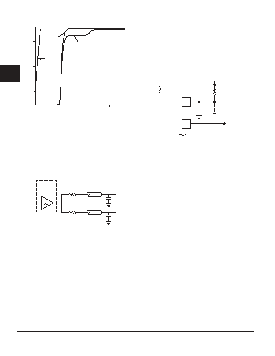
Figure 4. Single versus Dual Waveforms
TIME (nS)
VOL
TAGE
(V)
3.0
2.5
2.0
1.5
1.0
0.5
0
2
4
6
8
10
12
14
OutB
tD = 3.9386
OutA
tD = 3.8956
In
Since this step is well above the threshold region it will not
cause any false clock triggering, however designers may be
uncomfortable with unwanted reflections on the line. To better
match the impedances when driving multiple lines the situation
in Figure 5 should be used. In this case the series terminating
resistors are reduced such that when the parallel combination
is added to the output buffer impedance the line impedance is
perfectly matched.
Figure 5. Optimized Dual Line Termination
7
MPC9952
OUTPUT
BUFFER
RS = 36
ZO = 50
RS = 36
ZO = 50
7
+ 36 k 36 = 50 k 50
25
= 25
Power Supply Filtering
The MPC9952 is a mixed analog/digital product and as such
it exhibits some sensitivities that would not necessarily be
seen on a fully digital product. Analog circuitry is naturally sus-
ceptible to random noise, especially if this noise is seen on the
power supply pins. The MPC9952 provides separate power
supplies for the output buffers (VCCO) and the internal PLL
(VCCA) of the device. The purpose of this design technique is
to try and isolate the high switching noise digital outputs from
the relatively sensitive internal analog phase–locked loop. In a
controlled environment such as an evaluation board this level
of isolation is sufficient. However, in a digital system environ-
ment where it is more difficult to minimize noise on the power
supplies a second level of isolation may be required. The sim-
plest form of isolation is a power supply filter on the VCCA pin
for the MPC9952.
Figure 6. Power Supply Filter
VCCA
VCC
MPC9952
0.01F
22F
0.01F
3.3V
RS=5-15
Figure 6 illustrates a typical power supply filter scheme. The
MPC9952 is most susceptible to noise with spectral content in
the 1KHz to 1MHz range. Therefore the filter should be de-
signed to target this range. The key parameter that needs to be
met in the final filter design is the DC voltage drop that will be
seen between the VCC supply and the VCCA pin of the
MPC9952. From the data sheet the IVCCA current (the current
sourced through the VCCA pin) is typically 15mA (20mA maxi-
mum), assuming that a minimum of 3.3V – 5% must be main-
tained on the VCCA pin very little DC voltage drop can be toler-
ated when a 3.3V VCC supply is used. The resistor shown in
Figure 6 must have a resistance of 5–15
to meet the voltage
drop criteria. The RC filter pictured will provide a broadband
filter with approximately 100:1 attenuation for noise whose
spectral content is above 20KHz. As the noise frequency
crosses the series resonant point of an individual capacitor it’s
overall impedance begins to look inductive and thus increases
with increasing frequency. The parallel capacitor combination
shown ensures that a low impedance path to ground exists for
frequencies well above the bandwidth of the PLL.
Although the MPC9952 has several design features to mini-
mize the susceptibility to power supply noise (isolated power
and grounds and fully differential PLL) there still may be ap-
plications in which overall performance is being degraded due
to system power supply noise. The power supply filter
schemes discussed in this section should be adequate to elim-
inate power supply noise related problems in most designs.
2
相关PDF资料 |
PDF描述 |
|---|---|
| MPC9993ACR2 | 9993 SERIES, PLL BASED CLOCK DRIVER, 5 TRUE OUTPUT(S), 0 INVERTED OUTPUT(S), PQFP32 |
| MPC9993AC | 9993 SERIES, PLL BASED CLOCK DRIVER, 5 TRUE OUTPUT(S), 0 INVERTED OUTPUT(S), PQFP32 |
| MSFLDL-TTL-200 | ACTIVE DELAY LINE, TRUE OUTPUT, SIP4 |
| MSFLDL-TTL-19 | ACTIVE DELAY LINE, TRUE OUTPUT, SIP4 |
| MSFLDL-TTL-21 | ACTIVE DELAY LINE, TRUE OUTPUT, SIP4 |
相关代理商/技术参数 |
参数描述 |
|---|---|
| MPC9992 | 制造商:MOTOROLA 制造商全称:Motorola, Inc 功能描述:3.3 DIFFRERENTIAL ECL/PECL PLL CLOCK GENERATOR |
| MPC9992AC | 功能描述:时钟发生器及支持产品 RoHS:否 制造商:Silicon Labs 类型:Clock Generators 最大输入频率:14.318 MHz 最大输出频率:166 MHz 输出端数量:16 占空比 - 最大:55 % 工作电源电压:3.3 V 工作电源电流:1 mA 最大工作温度:+ 85 C 安装风格:SMD/SMT 封装 / 箱体:QFN-56 |
| MPC9992ACR2 | 功能描述:时钟发生器及支持产品 RoHS:否 制造商:Silicon Labs 类型:Clock Generators 最大输入频率:14.318 MHz 最大输出频率:166 MHz 输出端数量:16 占空比 - 最大:55 % 工作电源电压:3.3 V 工作电源电流:1 mA 最大工作温度:+ 85 C 安装风格:SMD/SMT 封装 / 箱体:QFN-56 |
| MPC9992FA | 功能描述:锁相环 - PLL 2.5 3.3V 400MHz Clock Generator RoHS:否 制造商:Silicon Labs 类型:PLL Clock Multiplier 电路数量:1 最大输入频率:710 MHz 最小输入频率:0.002 MHz 输出频率范围:0.002 MHz to 808 MHz 电源电压-最大:3.63 V 电源电压-最小:1.71 V 最大工作温度:+ 85 C 最小工作温度:- 40 C 封装 / 箱体:QFN-36 封装:Tray |
| MPC9992FAR2 | 制造商:Integrated Device Technology Inc 功能描述:PLL Clock Driver Single 32-Pin LQFP T/R |
发布紧急采购,3分钟左右您将得到回复。