参数资料
| 型号: | MR25H10CDC |
| 厂商: | Everspin Technologies Inc |
| 文件页数: | 4/20页 |
| 文件大小: | 0K |
| 描述: | IC MRAM 1MBIT 40MHZ 8DFN |
| 标准包装: | 570 |
| 格式 - 存储器: | RAM |
| 存储器类型: | MRAM(磁阻 RAM) |
| 存储容量: | 1M (128K x 8) |
| 速度: | 40MHz |
| 接口: | SPI 串行 |
| 电源电压: | 2.7 V ~ 3.6 V |
| 工作温度: | -40°C ~ 85°C |
| 封装/外壳: | 8-VDFN 裸露焊盘 |
| 供应商设备封装: | 8-DFN-EP,大型标志(5x6) |
| 包装: | 托盘 |
| 其它名称: | 819-1014 |
�� �
�
�MR25H10�
�2.� SPI� COMMUNICATIONS� PROTOCOL�
�MR25H10 can be operated in either SPI Mode 0 (CPOL=0, CPHA =0) or SPI Mode 3 (CPOL=1, CPHA=1). For �
�both modes, inputs are captured on the rising edge of the clock and data outputs occur on the falling �
�edge of the clock. When not conveying data, SCK remains low for Mode 0; while in Mode 3, SCK is high. The �
�memory determines the mode of operation (Mode 0 or Mode 3) based upon the state of the SCK when CS �
�falls.�
�All memory transactions start when CS is brought low to the memory. The first byte is a command code. De-�
�pending upon the command, subsequent bytes of address are input. Data is either input or output. There �
�is only one command performed per CS active period. CS must go inactive before another command can �
�be accepted. To ensure proper part operation according to specifications, it is necessary to terminate each �
�access by raising CS at the end of a byte (a multiple of 8 clock cycles from CS dropping) to avoid partial or �
�aborted accesses.�
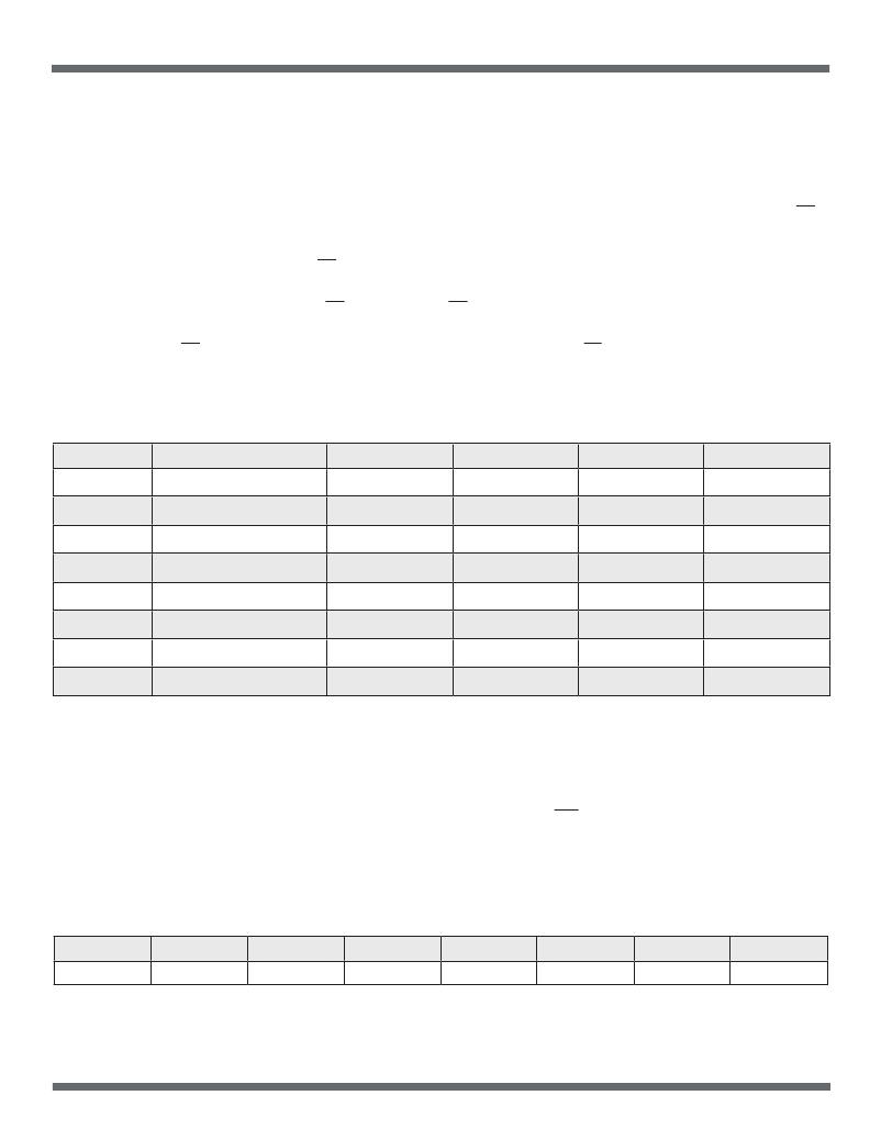
�Table� 2.1� Command� Codes�
�WREN�
�0000� 0110�
�Instruction�
� �
�WRDI� �
�RDSR �
�WRSR �
�READ� �
�WRITE �
�SLEEP �
�WAKE �
�Description�
�Write Enable �
�Write Disable� �
�Read Status Register �
�Write Status Register �
�Read Data Bytes �
�Write Data Bytes �
�Enter Sleep Mode �
�Exit Sleep Mode �
�Binary� Code�
� � �
�0000� � 0100� �
�0000 0101 �
�0000 0001 �
�0000� � 0011� �
�0000 0010 �
�1011 1001 �
�1010 1011 �
�Hex� Code�
�06h� �
�04h� �
�05h� �
�01h� �
�03h� �
�02h� �
�B9h� �
�ABh� �
�Address� Bytes�
�0 �
�0 �
�0 �
�0 �
�3�
�3�
�0 �
�0 �
�Data� Bytes�
�0 �
�0 �
�1 �
�1 �
�1 to ∞ �
�1 to ∞ �
�0 �
�0 �
�Status� Register� and� Block� Write� Protection�
�The status register consists of the 8 bits listed in table 2.2. Status register bits BP0 and BP1 define the mem-�
�ory block arrays that are protected as described in table 2.3. The Status Register Write Disable bit (SRWD) �
�is used in conjunction with bit 1 (WEL) and the Write Protection pin (WP) as shown in table 2.4 to enable �
�writes to status register bits. The fast writing speed of MR25H10 does not require write status bits. The �
�state of bits 6,5,4, and 0 can be user modified and do not affect memory operation. All bits in the status �
�register are pre-set from the factory to the “0” state.�
�Table� 2.2� Status� Register� Bit� Assignments�
�Bit� 7�
�SRWD�
�Bit� 6�
�Don’t Care�
�Bit� 5�
�Don’t Care�
�Bit� 4�
�Don’t Care�
�Bit� 3�
�BP1�
�Bit� 2�
�BP0�
�Bit� 1�
�WEL�
�Bit� 0�
�Don’t Care�
�Copyright� ?� Everspin� Technologies� 2013�
�4�
�MR25H10� Rev.� 9,� 4/2013�
�相关PDF资料 |
PDF描述 |
|---|---|
| 5747100-7 | CONN BACKSHELL DB37 METAL PLATED |
| FMC20DRYH | CONN EDGECARD 40POS DIP .100 SLD |
| MR256A08BCYS35 | IC MRAM 256KB 35NS 44TSOP |
| EPF10K30EQC208-1X | IC FLEX 10KE FPGA 30K 208-PQFP |
| AX500-2PQG208 | IC FPGA AXCELERATOR 500K 208QFP |
相关代理商/技术参数 |
参数描述 |
|---|---|
| MR25H10CDCR | 功能描述:NVRAM 1Mb 3.3V 128Kx8 Serial MRAM RoHS:否 制造商:Maxim Integrated 数据总线宽度:8 bit 存储容量:1024 Kbit 组织:128 K x 8 接口类型:Parallel 访问时间:70 ns 电源电压-最大:5.5 V 电源电压-最小:4.5 V 工作电流:85 mA 最大工作温度:+ 70 C 最小工作温度:0 C 封装 / 箱体:EDIP 封装:Tube |
| MR25H10CDF | 功能描述:NVRAM 1Mb 3.3V 128Kx8 Serial MRAM RoHS:否 制造商:Maxim Integrated 数据总线宽度:8 bit 存储容量:1024 Kbit 组织:128 K x 8 接口类型:Parallel 访问时间:70 ns 电源电压-最大:5.5 V 电源电压-最小:4.5 V 工作电流:85 mA 最大工作温度:+ 70 C 最小工作温度:0 C 封装 / 箱体:EDIP 封装:Tube |
| MR25H10CDFR | 功能描述:NVRAM 1Mb 3.3V 128Kx8 Serial MRAM RoHS:否 制造商:Maxim Integrated 数据总线宽度:8 bit 存储容量:1024 Kbit 组织:128 K x 8 接口类型:Parallel 访问时间:70 ns 电源电压-最大:5.5 V 电源电压-最小:4.5 V 工作电流:85 mA 最大工作温度:+ 70 C 最小工作温度:0 C 封装 / 箱体:EDIP 封装:Tube |
| MR25H10MDC | 功能描述:NVRAM 1Mb 3V 128Kx8 Serial MRAM RoHS:否 制造商:Maxim Integrated 数据总线宽度:8 bit 存储容量:1024 Kbit 组织:128 K x 8 接口类型:Parallel 访问时间:70 ns 电源电压-最大:5.5 V 电源电压-最小:4.5 V 工作电流:85 mA 最大工作温度:+ 70 C 最小工作温度:0 C 封装 / 箱体:EDIP 封装:Tube |
| MR25H10MDCR | 功能描述:NVRAM 1Mb 3V 128Kx8 Serial MRAM RoHS:否 制造商:Maxim Integrated 数据总线宽度:8 bit 存储容量:1024 Kbit 组织:128 K x 8 接口类型:Parallel 访问时间:70 ns 电源电压-最大:5.5 V 电源电压-最小:4.5 V 工作电流:85 mA 最大工作温度:+ 70 C 最小工作温度:0 C 封装 / 箱体:EDIP 封装:Tube |
发布紧急采购,3分钟左右您将得到回复。