- 您现在的位置:买卖IC网 > PDF目录80479 > MSP430F5509IRGZR (TEXAS INSTRUMENTS INC) 16-BIT, FLASH, 25 MHz, RISC MICROCONTROLLER, PQCC48 PDF资料下载
参数资料
| 型号: | MSP430F5509IRGZR |
| 厂商: | TEXAS INSTRUMENTS INC |
| 元件分类: | 微控制器/微处理器 |
| 英文描述: | 16-BIT, FLASH, 25 MHz, RISC MICROCONTROLLER, PQCC48 |
| 封装: | PLASTIC, VQFN-48 |
| 文件页数: | 12/99页 |
| 文件大小: | 1134K |
| 代理商: | MSP430F5509IRGZR |
第1页第2页第3页第4页第5页第6页第7页第8页第9页第10页第11页当前第12页第13页第14页第15页第16页第17页第18页第19页第20页第21页第22页第23页第24页第25页第26页第27页第28页第29页第30页第31页第32页第33页第34页第35页第36页第37页第38页第39页第40页第41页第42页第43页第44页第45页第46页第47页第48页第49页第50页第51页第52页第53页第54页第55页第56页第57页第58页第59页第60页第61页第62页第63页第64页第65页第66页第67页第68页第69页第70页第71页第72页第73页第74页第75页第76页第77页第78页第79页第80页第81页第82页第83页第84页第85页第86页第87页第88页第89页第90页第91页第92页第93页第94页第95页第96页第97页第98页第99页
PRODUCTPREVIEW
MSP430F550x
SLAS645B – JULY 2009 – REVISED JULY 2010
www.ti.com
DESCRIPTION
The Texas Instruments MSP430 family of ultralow-power microcontrollers consists of several devices featuring
different sets of peripherals targeted for various applications. The architecture, combined with extensive
low-power modes, is optimized to achieve extended battery life in portable measurement applications. The
device features a powerful 16-bit RISC CPU, 16-bit registers, and constant generators that contribute to
maximum code efficiency. The digitally controlled oscillator (DCO) allows wake-up from low-power modes to
active mode in less than 5 s.
The MSP430F5510, MSP430F5509, MSP430F5508 devices are microcontroller configurations with integrated
USB and PHY supporting USB 2.0, four 16-bit timers, a high-performance 10-bit analog-to-digital converter
(ADC), two universal serial communication interfaces (USCI), hardware multiplier, DMA, real-time clock module
with alarm capabilities, and 31 or 47 I/O pins.
The MSP430F5507, MSP430F5506, MSP430F5505, MSP430F5504 devices are configurations with integrated
USB and PHY supporting USB 2.0, four 16-bit timers, a high-performance 10-bit analog-to-digital converter
(ADC), two universal serial communication interfaces (USCI), hardware multiplier, DMA, real-time clock module
with alarm capabilities, and 31 I/O pins. The MSP430F5503, MSP430F5502, and MSP430FF5513 include all of
these peripherals but have a comparator instead of the 10-bit ADC.
Typical applications include analog and digital sensor systems, data loggers, etc., that require connectivity to
various USB hosts.
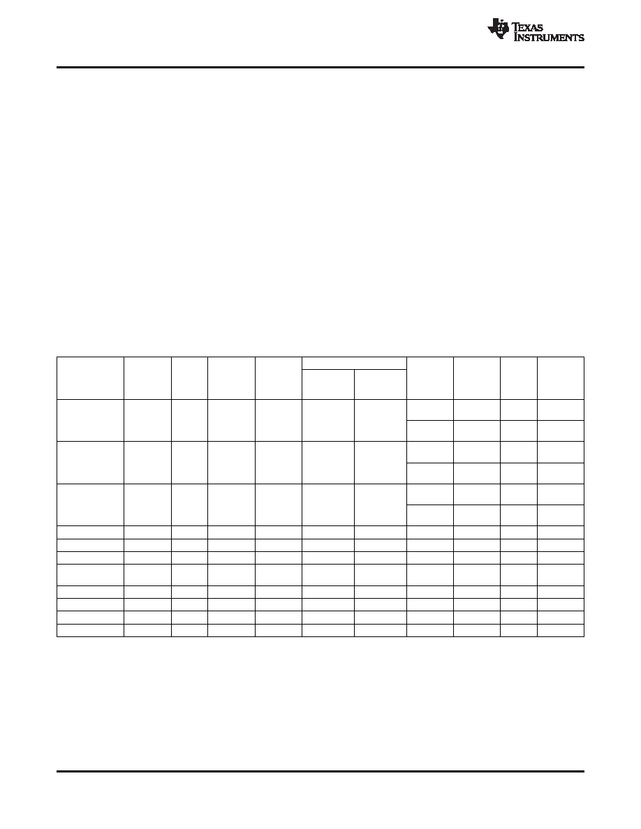
Family members available are summarized in Table 1.
Table 1. Family Members
USCI
PROGRAM
SRAM
ADC10_A
Comp_B
PACKAGE
CHANNEL A: CHANNEL B:
DEVICE
MEMORY
Timer_A(2)
Timer_B(3)
I/O
(KB)(1)
(CH)
TYPE
UART/LIN/Ir
SPI/ I2C
(KB)
DA/SPI
64 RGC,
10 ext / 2 int
8
47
80 ZQE
MSP430F5510
32
4 + 2
5, 3, 3
7
2
48 PT,
6 ext / 2 int
4
31
48 RGZ
64 RGC,
10 ext / 2 int
8
47
80 ZQE
MSP430F5509
24
4 + 2
5, 3, 3
7
2
48 PT,
6 ext / 2 int
4
31
48 RGZ,
64 RGC,
10 ext / 2 int
8
47
80 ZQE
MSP430F5508
16
4 + 2
5, 3, 3
7
2
48 PT,
6 ext / 2 int
4
31
48 RGZ,
MSP430F5507
32
4 + 2
5, 3, 3
7
1
6 ext / 2 int
-
31
48 RGZ
MSP430F5506
24
4 + 2
5, 3, 3
7
1
6 ext / 2 int
-
31
48 RGZ
MSP430F5505
16
4 + 2
5, 3, 3
7
1
6 ext / 2 int
-
31
48 RGZ
48 PT,
MSP430F5504
8
4 + 2
5, 3, 3
7
1
6 ext / 2 int
-
31
48 RGZ
MSP430F5503
32
4 + 2
5, 3, 3
7
1
-
4
31
48 RGZ
MSP430F5502
24
4 + 2
5, 3, 3
7
1
-
4
31
48 RGZ
MSP430F5501
16
4 + 2
5, 3, 3
7
1
-
4
31
48 RGZ
MSP430F5500
8
4 + 2
5, 3, 3
7
1
-
4
31
48 RGZ
(1)
The additional 2-KB USB SRAM that is listed can be used as general purpose SRAM when USB is not in use.
(2)
Each number in the sequence represents an instantiation of Timer_A with its associated number of capture compare registers and PWM
output generators available. For example, a number sequence of 3, 5 would represent two instantiations of Timer_A, the first
instantiation having 3 and the second instantiation having 5 capture compare registers and PWM output generators, respectively.
(3)
Each number in the sequence represents an instantiation of Timer_B with its associated number of capture compare registers and PWM
output generators available. For example, a number sequence of 3, 5 would represent two instantiations of Timer_B, the first
instantiation having 3 and the second instantiation having 5 capture compare registers and PWM output generators, respectively.
2
Copyright 2009–2010, Texas Instruments Incorporated
相关PDF资料 |
PDF描述 |
|---|---|
| MSP430F5510IZQE | 16-BIT, FLASH, 25 MHz, RISC MICROCONTROLLER, PBGA80 |
| MSP430G2221IPW14R | 16-BIT, FLASH, RISC MICROCONTROLLER, PDSO14 |
| MC68HLC908QT4CFQ | 8-BIT, FLASH, 2 MHz, MICROCONTROLLER, PQCC8 |
| MC68HLC908QY1CDT | 8-BIT, FLASH, 2 MHz, MICROCONTROLLER, PDSO16 |
| MC68HC11F1CFN2R2 | 8-BIT, EEPROM, 2 MHz, MICROCONTROLLER, PQCC68 |
相关代理商/技术参数 |
参数描述 |
|---|---|
| MSP430F5509IRGZT | 功能描述:16位微控制器 - MCU Mixed Signal MCU RoHS:否 制造商:Texas Instruments 核心:RISC 处理器系列:MSP430FR572x 数据总线宽度:16 bit 最大时钟频率:24 MHz 程序存储器大小:8 KB 数据 RAM 大小:1 KB 片上 ADC:Yes 工作电源电压:2 V to 3.6 V 工作温度范围:- 40 C to + 85 C 封装 / 箱体:VQFN-40 安装风格:SMD/SMT |
| MSP430F5509IZQE | 功能描述:16位微控制器 - MCU Mixed Signal MCU RoHS:否 制造商:Texas Instruments 核心:RISC 处理器系列:MSP430FR572x 数据总线宽度:16 bit 最大时钟频率:24 MHz 程序存储器大小:8 KB 数据 RAM 大小:1 KB 片上 ADC:Yes 工作电源电压:2 V to 3.6 V 工作温度范围:- 40 C to + 85 C 封装 / 箱体:VQFN-40 安装风格:SMD/SMT |
| MSP430F5509IZQER | 功能描述:16位微控制器 - MCU Mixed Signal MCU RoHS:否 制造商:Texas Instruments 核心:RISC 处理器系列:MSP430FR572x 数据总线宽度:16 bit 最大时钟频率:24 MHz 程序存储器大小:8 KB 数据 RAM 大小:1 KB 片上 ADC:Yes 工作电源电压:2 V to 3.6 V 工作温度范围:- 40 C to + 85 C 封装 / 箱体:VQFN-40 安装风格:SMD/SMT |
| MSP430F5510CY | 制造商:Texas Instruments 功能描述:IC MCU 16BIT 32KB FLASH DIE 制造商:Texas Instruments 功能描述:MSP430F5509 - DIE SALES |
| MSP430F5510CYS | 制造商:Texas Instruments 功能描述:IC MCU 16BIT 32KB FLASH DIE 制造商:Texas Instruments 功能描述:MSP430F5509 - WAFER SALES |
发布紧急采购,3分钟左右您将得到回复。