- 您现在的位置:买卖IC网 > PDF目录80479 > MSP430F5509IRGZR (TEXAS INSTRUMENTS INC) 16-BIT, FLASH, 25 MHz, RISC MICROCONTROLLER, PQCC48 PDF资料下载
参数资料
| 型号: | MSP430F5509IRGZR |
| 厂商: | TEXAS INSTRUMENTS INC |
| 元件分类: | 微控制器/微处理器 |
| 英文描述: | 16-BIT, FLASH, 25 MHz, RISC MICROCONTROLLER, PQCC48 |
| 封装: | PLASTIC, VQFN-48 |
| 文件页数: | 16/99页 |
| 文件大小: | 1134K |
| 代理商: | MSP430F5509IRGZR |
第1页第2页第3页第4页第5页第6页第7页第8页第9页第10页第11页第12页第13页第14页第15页当前第16页第17页第18页第19页第20页第21页第22页第23页第24页第25页第26页第27页第28页第29页第30页第31页第32页第33页第34页第35页第36页第37页第38页第39页第40页第41页第42页第43页第44页第45页第46页第47页第48页第49页第50页第51页第52页第53页第54页第55页第56页第57页第58页第59页第60页第61页第62页第63页第64页第65页第66页第67页第68页第69页第70页第71页第72页第73页第74页第75页第76页第77页第78页第79页第80页第81页第82页第83页第84页第85页第86页第87页第88页第89页第90页第91页第92页第93页第94页第95页第96页第97页第98页第99页
PRODUCTPREVIEW
MSP430F550x
www.ti.com
SLAS645B – JULY 2009 – REVISED JULY 2010
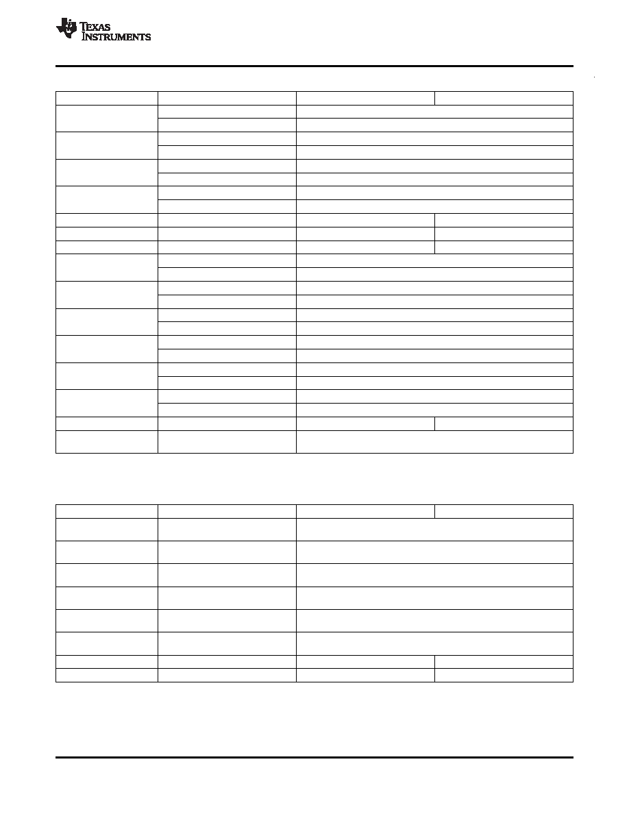
Table 9. Port Mapping, Mnemonics and Functions (continued)
VALUE
PxMAPy MNEMONIC
INPUT PIN FUNCTION
OUTPUT PIN FUNCTION
PM_UCA1CLK
USCI_A1 clock input/output (direction controlled by USCI)
13
PM_UCB1STE
USCI_B1 SPI slave transmit enable (direction controlled by USCI)
PM_UCB1SOMI
USCI_B1 SPI slave out master in (direction controlled by USCI)
14
PM_UCB1SCL
USCI_B1 I2C clock (open drain and direction controlled by USCI)
PM_UCB1SIMO
USCI_B1 SPI slave in master out (direction controlled by USCI)
15
PM_UCB1SDA
USCI_B1 I2C data (open drain and direction controlled by USCI)
PM_UCB1CLK
USCI_B1 clock input/output (direction controlled by USCI)
16
PM_UCA1STE
USCI_A1 SPI slave transmit enable (direction controlled by USCI)
17
PM_CBOUT1
None
Comparator_B output
18
PM_MCLK
None
MCLK
19
PM_RTCCLK
None
RTCCLK output
PM_UCA0RXD
USCI_A0 UART RXD (Direction controlled by USCI - input)
20
PM_UCA0SOMI
USCI_A0 SPI slave out master in (direction controlled by USCI)
PM_UCA0TXD
USCI_A0 UART TXD (Direction controlled by USCI - output)
21
PM_UCA0SIMO
USCI_A0 SPI slave in master out (direction controlled by USCI)
PM_UCA0CLK
USCI_A0 clock input/output (direction controlled by USCI)
22
PM_UCB0STE
USCI_B0 SPI slave transmit enable (direction controlled by USCI)
PM_UCB0SOMI
USCI_B0 SPI slave out master in (direction controlled by USCI)
23
PM_UCB0SCL
USCI_B0 I2C clock (open drain and direction controlled by USCI)
PM_UCB0SIMO
USCI_B0 SPI slave in master out (direction controlled by USCI)
24
PM_UCB0SDA
USCI_B0 I2C data (open drain and direction controlled by USCI)
PM_UCB0CLK
USCI_B0 clock input/output (direction controlled by USCI)
25
PM_UCA0STE
USCI_A0 SPI slave transmit enable (direction controlled by USCI)
26 - 30
Reserved
None
DVSS
Disables the output driver as well as the input Schmitt-trigger to prevent
31 (0FFh)(1)
PM_ANALOG
parasitic cross currents when applying analog signals.
(1)
The value of the PMPAP_ANALOG mnemonic is set to 0FFh. The port mapping registers are only 5 bits wide and the upper bits are
ignored resulting in a read out value of 31.
Table 10. Default Mapping
PIN
PxMAPy MNEMONIC
INPUT PIN FUNCTION
OUTPUT PIN FUNCTION
USCI_B1 SPI slave transmit enable (direction controlled by USCI)
P4.0/P4MAP0
PM_UCB1STE/PM_UCA1CLK
USCI_A1 clock input/output (direction controlled by USCI)
USCI_B1 SPI slave in master out (direction controlled by USCI)
P4.1/P4MAP1
PM_UCB1SIMO/PM_UCB1SDA
USCI_B1 I2C data (open drain and direction controlled by USCI)
USCI_B1 SPI slave out master in (direction controlled by USCI)
P4.2/P4MAP2
PM_UCB1SOMI/PM_UCB1SCL
USCI_B1 I2C clock (open drain and direction controlled by USCI)
USCI_A1 SPI slave transmit enable (direction controlled by USCI)
P4.3/P4MAP3
PM_UCB1CLK/PM_UCA1STE
USCI_B1 clock input/output (direction controlled by USCI)
USCI_A1 UART TXD (Direction controlled by USCI - output)
P4.4/P4MAP4
PM_UCA1TXD/PM_UCA1SIMO
USCI_A1 SPI slave in master out (direction controlled by USCI)
USCI_A1 UART RXD (Direction controlled by USCI - input)
P4.5/P4MAP5
PM_UCA1RXD/PM_UCA1SOMI
USCI_A1 SPI slave out master in (direction controlled by USCI)
P4.6/P4MAP6
PM_NONE
None
DVSS
P4.7/P4MAP7
PM_NONE
None
DVSS
Copyright 2009–2010, Texas Instruments Incorporated
23
相关PDF资料 |
PDF描述 |
|---|---|
| MSP430F5510IZQE | 16-BIT, FLASH, 25 MHz, RISC MICROCONTROLLER, PBGA80 |
| MSP430G2221IPW14R | 16-BIT, FLASH, RISC MICROCONTROLLER, PDSO14 |
| MC68HLC908QT4CFQ | 8-BIT, FLASH, 2 MHz, MICROCONTROLLER, PQCC8 |
| MC68HLC908QY1CDT | 8-BIT, FLASH, 2 MHz, MICROCONTROLLER, PDSO16 |
| MC68HC11F1CFN2R2 | 8-BIT, EEPROM, 2 MHz, MICROCONTROLLER, PQCC68 |
相关代理商/技术参数 |
参数描述 |
|---|---|
| MSP430F5509IRGZT | 功能描述:16位微控制器 - MCU Mixed Signal MCU RoHS:否 制造商:Texas Instruments 核心:RISC 处理器系列:MSP430FR572x 数据总线宽度:16 bit 最大时钟频率:24 MHz 程序存储器大小:8 KB 数据 RAM 大小:1 KB 片上 ADC:Yes 工作电源电压:2 V to 3.6 V 工作温度范围:- 40 C to + 85 C 封装 / 箱体:VQFN-40 安装风格:SMD/SMT |
| MSP430F5509IZQE | 功能描述:16位微控制器 - MCU Mixed Signal MCU RoHS:否 制造商:Texas Instruments 核心:RISC 处理器系列:MSP430FR572x 数据总线宽度:16 bit 最大时钟频率:24 MHz 程序存储器大小:8 KB 数据 RAM 大小:1 KB 片上 ADC:Yes 工作电源电压:2 V to 3.6 V 工作温度范围:- 40 C to + 85 C 封装 / 箱体:VQFN-40 安装风格:SMD/SMT |
| MSP430F5509IZQER | 功能描述:16位微控制器 - MCU Mixed Signal MCU RoHS:否 制造商:Texas Instruments 核心:RISC 处理器系列:MSP430FR572x 数据总线宽度:16 bit 最大时钟频率:24 MHz 程序存储器大小:8 KB 数据 RAM 大小:1 KB 片上 ADC:Yes 工作电源电压:2 V to 3.6 V 工作温度范围:- 40 C to + 85 C 封装 / 箱体:VQFN-40 安装风格:SMD/SMT |
| MSP430F5510CY | 制造商:Texas Instruments 功能描述:IC MCU 16BIT 32KB FLASH DIE 制造商:Texas Instruments 功能描述:MSP430F5509 - DIE SALES |
| MSP430F5510CYS | 制造商:Texas Instruments 功能描述:IC MCU 16BIT 32KB FLASH DIE 制造商:Texas Instruments 功能描述:MSP430F5509 - WAFER SALES |
发布紧急采购,3分钟左右您将得到回复。