- 您现在的位置:买卖IC网 > PDF目录379326 > MTB23P06 (Motorola, Inc.) TMOS POWER FET 23 AMPERES 60 VOLTS PDF资料下载
参数资料
| 型号: | MTB23P06 |
| 厂商: | Motorola, Inc. |
| 英文描述: | TMOS POWER FET 23 AMPERES 60 VOLTS |
| 中文描述: | TMOS是功率FET 23安培60伏特 |
| 文件页数: | 4/10页 |
| 文件大小: | 280K |
| 代理商: | MTB23P06 |
4
Motorola TMOS Power MOSFET Transistor Device Data
POWER MOSFET SWITCHING
Switching behavior is most easily modeled and predicted
by recognizing that the power MOSFET is charge controlled.
The lengths of various switching intervals (
t) are deter-
mined by how fast the FET input capacitance can be charged
by current from the generator.
The published capacitance data is difficult to use for calculat-
ing rise and fall because drain–gate capacitance varies
greatly with applied voltage. Accordingly, gate charge data is
used. In most cases, a satisfactory estimate of average input
current (IG(AV)) can be made from a rudimentary analysis of
the drive circuit so that
t = Q/IG(AV)
During the rise and fall time interval when switching a resis-
tive load, VGS remains virtually constant at a level known as
the plateau voltage, VSGP. Therefore, rise and fall times may
be approximated by the following:
tr = Q2 x RG/(VGG – VGSP)
tf = Q2 x RG/VGSP
where
VGG = the gate drive voltage, which varies from zero to VGG
RG = the gate drive resistance
and Q2 and VGSP are read from the gate charge curve.
During the turn–on and turn–off delay times, gate current is
not constant. The simplest calculation uses appropriate val-
ues from the capacitance curves in a standard equation for
voltage change in an RC network. The equations are:
td(on) = RG Ciss In [VGG/(VGG – VGSP)]
td(off) = RG Ciss In (VGG/VGSP)
The capacitance (Ciss) is read from the capacitance curve at
a voltage corresponding to the off–state condition when cal-
culating td(on) and is read at a voltage corresponding to the
on–state when calculating td(off).
At high switching speeds, parasitic circuit elements com-
plicate the analysis. The inductance of the MOSFET source
lead, inside the package and in the circuit wiring which is
common to both the drain and gate current paths, produces a
voltage at the source which reduces the gate drive current.
The voltage is determined by Ldi/dt, but since di/dt is a func-
tion of drain current, the mathematical solution is complex.
The MOSFET output capacitance also complicates the
mathematics. And finally, MOSFETs have finite internal gate
resistance which effectively adds to the resistance of the
driving source, but the internal resistance is difficult to mea-
sure and, consequently, is not specified.
The resistive switching time variation versus gate resis-
tance (Figure 9) shows how typical switching performance is
affected by the parasitic circuit elements. If the parasitics
were not present, the slope of the curves would maintain a
value of unity regardless of the switching speed. The circuit
used to obtain the data is constructed to minimize common
inductance in the drain and gate circuit loops and is believed
readily achievable with board mounted components. Most
power electronic loads are inductive; the data in the figure is
taken with a resistive load, which approximates an optimally
snubbed inductive load. Power MOSFETs may be safely op-
erated into an inductive load; however, snubbing reduces
switching losses.
8000
7000
6000
5000
4000
3000
2000
1000
0
25
20
15
10
5
0
5
10
15
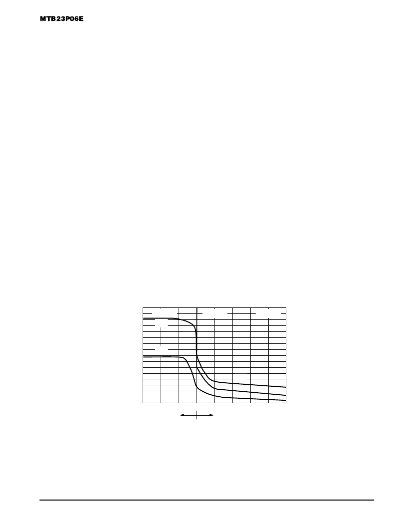
GATE–TO–SOURCE OR DRAIN–TO–SOURCE VOLTAGE (VOLTS)
C
TJ = 25
°
C
VGS = 0 V
VDS = 0 V
Ciss
Ciss
Crss
Coss
VGS
VDS
Crss
Figure 7. Capacitance Variation
相关PDF资料 |
PDF描述 |
|---|---|
| MTB23P06E | TMOS POWER FET 23 AMPERES 60 VOLTS |
| MTB23P06V | IC REG LDO 750MA ADJ TO263-5 |
| MTB50P03HDL | TMOS POWER FET LOGIC LEVEL 50 AMPERES 30 VOLTS |
| MTB75N03HDL | TMOS POWER FET LOGIC LEVEL 75 AMPERES 25 VOLTS |
| MTB8N50E | TMOS POWER FET 8.0 AMPERES 500 VOLTS |
相关代理商/技术参数 |
参数描述 |
|---|---|
| MTB23P06E | 制造商:MOTOROLA 制造商全称:Motorola, Inc 功能描述:TMOS POWER FET 23 AMPERES 60 VOLTS |
| MTB23P06ET4 | 制造商:Motorola Inc 功能描述: |
| MTB23P06V | 制造商:ON Semiconductor 功能描述:Trans MOSFET P-CH 60V 23A 3-Pin(2+Tab) D2PAK Rail |
| MTB23P06VT4 | 功能描述:MOSFET P-CH 60V 23A D2PAK RoHS:否 类别:分离式半导体产品 >> FET - 单 系列:- 标准包装:1,000 系列:MESH OVERLAY™ FET 型:MOSFET N 通道,金属氧化物 FET 特点:逻辑电平门 漏极至源极电压(Vdss):200V 电流 - 连续漏极(Id) @ 25° C:18A 开态Rds(最大)@ Id, Vgs @ 25° C:180 毫欧 @ 9A,10V Id 时的 Vgs(th)(最大):4V @ 250µA 闸电荷(Qg) @ Vgs:72nC @ 10V 输入电容 (Ciss) @ Vds:1560pF @ 25V 功率 - 最大:40W 安装类型:通孔 封装/外壳:TO-220-3 整包 供应商设备封装:TO-220FP 包装:管件 |
| MTB2-3PH001 | 制造商:ITT Interconnect Solutions 功能描述:MTB2-3PH001 - Bulk |
发布紧急采购,3分钟左右您将得到回复。