- 您现在的位置:买卖IC网 > PDF目录98046 > MTB60N06HDT4 (ON SEMICONDUCTOR) 60 A, 60 V, 0.014 ohm, N-CHANNEL, Si, POWER, MOSFET PDF资料下载
参数资料
| 型号: | MTB60N06HDT4 |
| 厂商: | ON SEMICONDUCTOR |
| 元件分类: | JFETs |
| 英文描述: | 60 A, 60 V, 0.014 ohm, N-CHANNEL, Si, POWER, MOSFET |
| 封装: | CASE 418B-03, D2PAK-3 |
| 文件页数: | 6/11页 |
| 文件大小: | 279K |
| 代理商: | MTB60N06HDT4 |
MTB60N06HD
http://onsemi.com
4
POWER MOSFET SWITCHING
Switching behavior is most easily modeled and predicted
by recognizing that the power MOSFET is charge
controlled. The lengths of various switching intervals (Δt)
are determined by how fast the FET input capacitance can
be charged by current from the generator.
The published capacitance data is difficult to use for
calculating rise and fall because draingate capacitance
varies greatly with applied voltage. Accordingly, gate
charge data is used. In most cases, a satisfactory estimate of
average input current (IG(AV)) can be made from a
rudimentary analysis of the drive circuit so that
t = Q/IG(AV)
During the rise and fall time interval when switching a
resistive load, VGS remains virtually constant at a level
known as the plateau voltage, VSGP. Therefore, rise and fall
times may be approximated by the following:
tr = Q2 x RG/(VGG VGSP)
tf = Q2 x RG/VGSP
where
VGG = the gate drive voltage, which varies from zero to VGG
RG = the gate drive resistance
and Q2 and VGSP are read from the gate charge curve.
During the turnon and turnoff delay times, gate current is
not constant. The simplest calculation uses appropriate
values from the capacitance curves in a standard equation for
voltage change in an RC network. The equations are:
td(on) = RG Ciss In [VGG/(VGG VGSP)]
td(off) = RG Ciss In (VGG/VGSP)
The capacitance (Ciss) is read from the capacitance curve at
a voltage corresponding to the offstate condition when
calculating td(on) and is read at a voltage corresponding to the
onstate when calculating td(off).
At high switching speeds, parasitic circuit elements
complicate the analysis. The inductance of the MOSFET
source lead, inside the package and in the circuit wiring
which is common to both the drain and gate current paths,
produces a voltage at the source which reduces the gate drive
current. The voltage is determined by Ldi/dt, but since di/dt
is a function of drain current, the mathematical solution is
complex. The MOSFET output capacitance also
complicates the mathematics. And finally, MOSFETs have
finite internal gate resistance which effectively adds to the
resistance of the driving source, but the internal resistance
is difficult to measure and, consequently, is not specified.
The resistive switching time variation versus gate
resistance (Figure 9) shows how typical switching
performance is affected by the parasitic circuit elements. If
the parasitics were not present, the slope of the curves would
maintain a value of unity regardless of the switching speed.
The circuit used to obtain the data is constructed to minimize
common inductance in the drain and gate circuit loops and
is believed readily achievable with board mounted
components. Most power electronic loads are inductive; the
data in the figure is taken with a resistive load, which
approximates an optimally snubbed inductive load. Power
MOSFETs may be safely operated into an inductive load;
however, snubbing reduces switching losses.
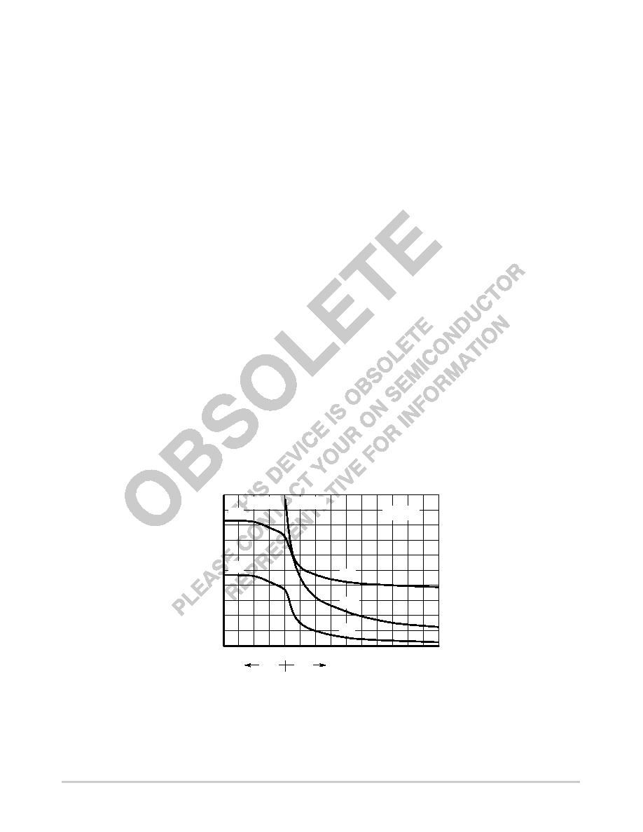
GATETOSOURCE OR DRAINTOSOURCE VOLTAGE (VOLTS)
C,
CAP
ACIT
ANCE
(pF)
0
1000
2000
3000
5000
Figure 7. Capacitance Variation
4000
10
0
10
15
20
25
VGS
VDS
55
VDS = 0 V
Ciss
Crss
VGS = 0 V
TJ = 25°C
Ciss
Coss
Crss
相关PDF资料 |
PDF描述 |
|---|---|
| MTB75N03HDL | 75 A, 25 V, 0.009 ohm, N-CHANNEL, Si, POWER, MOSFET |
| MTB75N03HDLT4 | 75 A, 25 V, 0.009 ohm, N-CHANNEL, Si, POWER, MOSFET |
| MTB75N06HDT4 | 75 A, 60 V, 0.01 ohm, N-CHANNEL, Si, POWER, MOSFET |
| MTB75N06HD | 75 A, 60 V, 0.01 ohm, N-CHANNEL, Si, POWER, MOSFET |
| MTB75N06HDT4 | 75 A, 60 V, 0.01 ohm, N-CHANNEL, Si, POWER, MOSFET |
相关代理商/技术参数 |
参数描述 |
|---|---|
| MTB60N06J3 | 制造商:CYSTEKEC 制造商全称:Cystech Electonics Corp. 功能描述:N -Channel Enhancement Mode Power MOSFET |
| MTB60N10E7L | 制造商:Rochester Electronics LLC 功能描述:- Bulk |
| MTB60N10E7LT4 | 制造商:Motorola Inc 功能描述: |
| MTB60P06H8 | 制造商:CYSTEKEC 制造商全称:Cystech Electonics Corp. 功能描述:P-Channel Logic Level Enhancement Mode Power MOSFET |
| MTB6N60 | 制造商:MOTOROLA 制造商全称:Motorola, Inc 功能描述:TMOS POWER FET 6.0 AMPERES 600 VOLTS |
发布紧急采购,3分钟左右您将得到回复。