- 您现在的位置:买卖IC网 > PDF目录96091 > MTB60N10E7L (MOTOROLA INC) 60 A, 100 V, 0.024 ohm, N-CHANNEL, Si, POWER, MOSFET PDF资料下载
参数资料
| 型号: | MTB60N10E7L |
| 厂商: | MOTOROLA INC |
| 元件分类: | JFETs |
| 英文描述: | 60 A, 100 V, 0.024 ohm, N-CHANNEL, Si, POWER, MOSFET |
| 封装: | D2PAK-3 |
| 文件页数: | 2/8页 |
| 文件大小: | 182K |
| 代理商: | MTB60N10E7L |
MTB60N10E7L
2
Motorola TMOS Power MOSFET Transistor Device Data
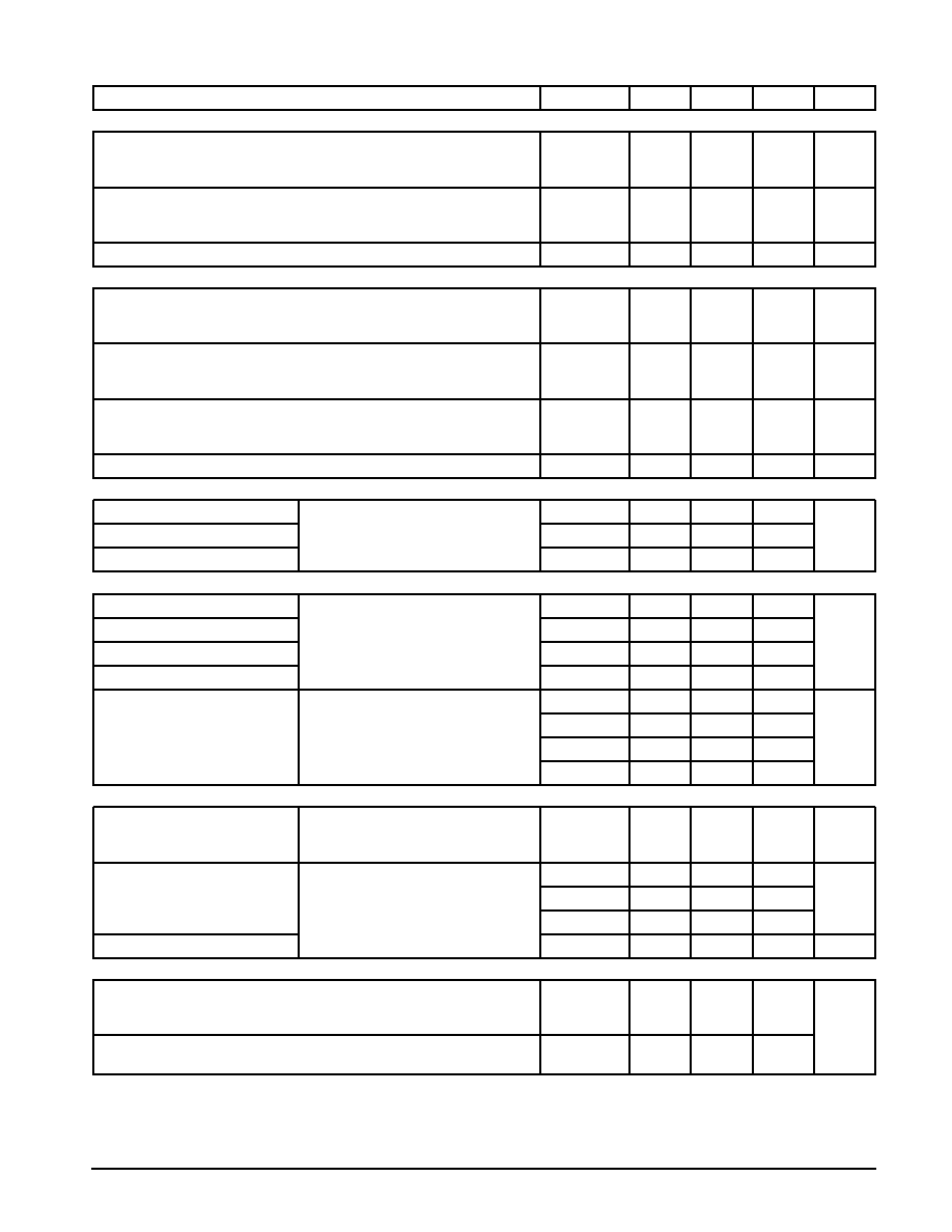
ELECTRICAL CHARACTERISTICS (TJ = 25°C unless otherwise noted)
Characteristic
Symbol
Min
Typ
Max
Unit
OFF CHARACTERISTICS
Drain–to–Source Breakdown Voltage
(VGS = 0 Vdc, ID = 0.25 mAdc)
Temperature Coefficient (Positive)
V(BR)DSS
100
—
135
—
Vdc
mV/
°C
Zero Gate Voltage Drain Current
(VDS = 100 Vdc, VGS = 0 Vdc)
(VDS = 100 Vdc, VGS = 0 Vdc, TJ =150°C)
IDSS
—
10
100
Adc
Gate–Body Leakage Current (VGS = ± 20 Vdc, VDS = 0 Vdc)
IGSS
—
100
nAdc
ON CHARACTERISTICS (1)
Gate Threshold Voltage
(VDS = VGS, ID = 250 Adc)
Threshold Temperature Coefficient (Negative)
VGS(th)
1.0
—
1.5
5.5
2.0
—
Vdc
mV/
°C
Static Drain–to–Source On–Resistance
(VGS = 10 Vdc, ID = 30 Adc)
(VGS = 5.0 Vdc, ID = 30 Adc)
RDS(on)
—
0.019
0.021
0.022
0.024
Ohms
Drain–to–Source On–Voltage
(VGS = 10 Vdc, ID = 60 Adc)
(VGS = 10 Vdc, ID = 30 Adc, TJ = 150°C)
VDS(on)
—
1.6
1.5
Vdc
Forward Transconductance (VDS = 8 Vdc, ID = 15 Adc)
gFS
30
35
—
mhos
DYNAMIC CHARACTERISTICS
Input Capacitance
(V
25 Vdc V
0 Vdc
Ciss
—
3000
4200
pF
Output Capacitance
(VDS = 25 Vdc, VGS = 0 Vdc,
f = 1.0 MHz)
Coss
—
625
880
Transfer Capacitance
f = 1.0 MHz)
Crss
—
140
280
SWITCHING CHARACTERISTICS (2)
Turn–On Delay Time
(V
50 Vd
I
30 Ad
td(on)
—
15
30
ns
Rise Time
(VDD = 50 Vdc, ID = 30 Adc,
VGS =5 0Vdc
tr
—
215
430
Turn–Off Delay Time
VGS = 5.0 Vdc,
RG = 1.4 )
td(off)
—
60
120
Fall Time
G
)
tf
—
130
260
Gate Charge
(See Figure 8)
(V
80 Vd
I
30 Ad
QT
—
67
90
nC
(See Figure 8)
(VDS = 80 Vdc, ID = 30 Adc,
Q1
—
10
—
( DS
, D
,
VGS = 5.0 Vdc)
Q2
—
42
—
Q3
—
36
—
SOURCE–DRAIN DIODE CHARACTERISTICS
Forward On–Voltage
(IS = 30 Adc, VGS = 0 Vdc)
(IS = 30 Adc, VGS = 0 Vdc, TJ = 150°C)
VSD
—
0.81
0.65
1.0
—
Vdc
Reverse Recovery Time
(See Figure 14)
(I
30 Ad
V
0 Vd
trr
—
155
—
ns
(See Figure 14)
(IS = 30 Adc, VGS = 0 Vdc,
ta
—
100
—
( S
,
GS
,
dIS/dt = 100 A/s)
tb
—
55
—
Reverse Recovery Stored Charge
QRR
—
0.87
—
C
INTERNAL PACKAGE INDUCTANCE
Internal Drain Inductance
(Measured from contact screw on tab to center of die)
(Measured from the drain lead 0.25
″ from package to center of die)
LD
—
3.5
4.5
—
nH
Internal Source Inductance
(Measured from the source lead 0.25
″ from package to source bond pad)
LS
—
7.5
—
(1) Pulse Test: Pulse Width
≤ 300 s, Duty Cycle ≤ 2%.
(2) Switching characteristics are independent of operating junction temperature.
相关PDF资料 |
PDF描述 |
|---|---|
| MTB60N10E7LT4 | 60 A, 100 V, 0.024 ohm, N-CHANNEL, Si, POWER, MOSFET |
| MTB71040L | 60 A, 100 V, 0.024 ohm, N-CHANNEL, Si, POWER, MOSFET |
| MTB71040LT4 | 60 A, 100 V, 0.024 ohm, N-CHANNEL, Si, POWER, MOSFET |
| MTB75N05HD | 75 A, 50 V, 0.0095 ohm, N-CHANNEL, Si, POWER, MOSFET |
| MTB75N05HDT4 | 75 A, 50 V, 0.0095 ohm, N-CHANNEL, Si, POWER, MOSFET |
相关代理商/技术参数 |
参数描述 |
|---|---|
| MTB60N10E7LT4 | 制造商:Motorola Inc 功能描述: |
| MTB60P06H8 | 制造商:CYSTEKEC 制造商全称:Cystech Electonics Corp. 功能描述:P-Channel Logic Level Enhancement Mode Power MOSFET |
| MTB6N60 | 制造商:MOTOROLA 制造商全称:Motorola, Inc 功能描述:TMOS POWER FET 6.0 AMPERES 600 VOLTS |
| MTB6N60E | 制造商:ON Semiconductor 功能描述: |
| MTB6N60E1 | 制造商:ON Semiconductor 功能描述: |
发布紧急采购,3分钟左右您将得到回复。