- 您现在的位置:买卖IC网 > PDF目录96091 > MTB60N10E7LT4 (MOTOROLA INC) 60 A, 100 V, 0.024 ohm, N-CHANNEL, Si, POWER, MOSFET PDF资料下载
参数资料
| 型号: | MTB60N10E7LT4 |
| 厂商: | MOTOROLA INC |
| 元件分类: | JFETs |
| 英文描述: | 60 A, 100 V, 0.024 ohm, N-CHANNEL, Si, POWER, MOSFET |
| 封装: | D2PAK-3 |
| 文件页数: | 1/8页 |
| 文件大小: | 182K |
| 代理商: | MTB60N10E7LT4 |
1
Motorola TMOS Power MOSFET Transistor Device Data
Advance Information
TMOS E-FET.
High Energy Power FET
D2PAK for Surface Mount
N–Channel Enhancement–Mode Silicon Gate
The D2PAK package has the capability of housing a larger die
than any existing surface mount package which allows it to be used
in applications that require the use of surface mount components
with higher power and lower RDS(on) capabilities. This advanced
TMOS E–FET is designed to withstand high energy in the
avalanche and commutation modes. This new energy efficient
design also offers a drain–to–source diode with a fast recovery
time. Designed for medium voltage, high speed switching applica-
tions in power supplies, converters and PWM motor controls.
These devices are particularly well suited for bridge circuits where
diode speed and commutating safe operating areas are critical and
offer additional safety margin against unexpected voltage tran-
sients.
New Features of TMOS 7
Ultra Low On–Resistance Provides Higher Efficiency
Reduced Gate Charge
Features Common to TMOS 7 and TMOS E–FETS
Logic Level Gate Drive
Avalanche Energy Specified
Diode Characterized for Use in Bridge Circuits
IDSS and VDS(on) Specified at Elevated Temperature
Industry Standard D2PAK Surface Mount Package
Surface Mount Package Available in 24 mm, 13–inch/800 Unit
Tape & Reel, Add T4 Suffix to Part Number
MAXIMUM RATINGS (TC = 25°C unless otherwise noted)
Rating
Symbol
Value
Unit
Drain–to–Source Voltage
VDSS
100
Vdc
Drain–to–Gate Voltage (RGS = 1.0 M)
VDGR
100
Vdc
Gate–to–Source Voltage — Continuous
Gate–to–Source Voltage — Non–Repetitive (tp ≤ 10 ms)
VGS
VGSM
± 20
± 25
Vdc
Vpk
Drain Current — Continuous
Drain Current — Continuous @ 100
°C
Drain Current — Single Pulse (tp ≤ 10 s)
ID
IDM
60
48
210
Adc
Apk
Total Power Dissipation
Derate above 25
°C
Total Power Dissipation @ TA = 25°C (1)
PD
242
1.61
3.0
Watts
W/
°C
Watts
Operating and Storage Temperature Range
TJ, Tstg
– 55 to 175
°C
Single Pulse Drain–to–Source Avalanche Energy — Starting TJ = 25°C
(VDD = 60 Vdc, VGS = 5.0 Vdc, PEAK IL = 60 Apk, L = 0.3 mH, RG = 25 )
EAS
540
mJ
Thermal Resistance — Junction to Case
Thermal Resistance — Junction to Ambient
Thermal Resistance — Junction to Ambient (1)
R
θJC
R
θJA
R
θJA
0.62
62.5
50
°C/W
Maximum Lead Temperature for Soldering Purposes, 1/8
″ from case for 10 seconds
TL
260
°C
(1) When surface mounted to an FR4 board using the minimum recommended pad size.
This document contains information on a new product. Specifications and information herein are subject to change without notice.
E–FET is a trademark of Motorola, Inc. TMOS is a registered trademark of Motorola, Inc.
Order this document
by MTB60N10E7L/D
MOTOROLA
SEMICONDUCTOR TECHNICAL DATA
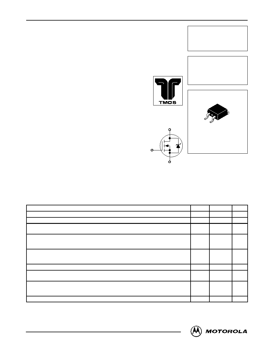
MTB60N10E7L
TMOS POWER FET
60 AMPERES
100 VOLTS
RDS(on) = 0.022 W
CASE 418B–03, Style 2
D2PAK
D
S
G
N–Channel
Motorola, Inc. 1999
相关PDF资料 |
PDF描述 |
|---|---|
| MTB71040L | 60 A, 100 V, 0.024 ohm, N-CHANNEL, Si, POWER, MOSFET |
| MTB71040LT4 | 60 A, 100 V, 0.024 ohm, N-CHANNEL, Si, POWER, MOSFET |
| MTB75N05HD | 75 A, 50 V, 0.0095 ohm, N-CHANNEL, Si, POWER, MOSFET |
| MTB75N05HDT4 | 75 A, 50 V, 0.0095 ohm, N-CHANNEL, Si, POWER, MOSFET |
| MTB8N50ET4 | 8 A, 500 V, 0.8 ohm, N-CHANNEL, Si, POWER, MOSFET |
相关代理商/技术参数 |
参数描述 |
|---|---|
| MTB60P06H8 | 制造商:CYSTEKEC 制造商全称:Cystech Electonics Corp. 功能描述:P-Channel Logic Level Enhancement Mode Power MOSFET |
| MTB6N60 | 制造商:MOTOROLA 制造商全称:Motorola, Inc 功能描述:TMOS POWER FET 6.0 AMPERES 600 VOLTS |
| MTB6N60E | 制造商:ON Semiconductor 功能描述: |
| MTB6N60E1 | 制造商:ON Semiconductor 功能描述: |
| MTB6N60ET4 | 制造商:Rochester Electronics LLC 功能描述:- Bulk 制造商:ON Semiconductor 功能描述: |
发布紧急采购,3分钟左右您将得到回复。