- 您现在的位置:买卖IC网 > Datasheet目录480 > MTD6N15T4 (ON Semiconductor)MOSFET N-CH 150V 6A DPAK Datasheet资料下载
参数资料
| 型号: | MTD6N15T4 |
| 厂商: | ON Semiconductor |
| 文件页数: | 4/6页 |
| 文件大小: | 0K |
| 描述: | MOSFET N-CH 150V 6A DPAK |
| 产品变化通告: | Product Obsolescence 21/Jan/2010 |
| 标准包装: | 10 |
| FET 型: | MOSFET N 通道,金属氧化物 |
| FET 特点: | 标准 |
| 漏极至源极电压(Vdss): | 150V |
| 电流 - 连续漏极(Id) @ 25° C: | 6A |
| 开态Rds(最大)@ Id, Vgs @ 25° C: | 300 毫欧 @ 3A,10V |
| Id 时的 Vgs(th)(最大): | 4.5V @ 1mA |
| 闸电荷(Qg) @ Vgs: | 30nC @ 10V |
| 输入电容 (Ciss) @ Vds: | 1200pF @ 25V |
| 功率 - 最大: | 1.25W |
| 安装类型: | 表面贴装 |
| 封装/外壳: | TO-252-3,DPak(2 引线+接片),SC-63 |
| 供应商设备封装: | DPAK-3 |
| 包装: | 标准包装 |
| 其它名称: | MTD6N15T4OSDKR |
�� �
�
�MTD6N15�
�SAFE� OPERATING� AREA�
�20�
�10�
�5�
�100� m� s�
�1� ms�
�10� m� s�
�20�
�15�
�2�
�1�
�0.5�
�10 ms�
�R� DS(on)� LIMIT�
�10�
�T� J� ≤� 150� °� C�
�THERMAL� LIMIT�
�0.2�
�0.1�
�0.05�
�PACKAGE� LIMIT�
�T� C� =� 25� °� C�
�V� GS� =� 20� V� SINGLE� PULSE�
�dc�
�5�
�0.03�
�0.3� 0.5� 0.7� 1�
�2�
�3�
�5� 7� 10�
�20� 30�
�50� 70� 100�
�200� 300�
�0�
�0�
�20�
�40� 60� 80� 100� 120� 140�
�160�
�V� DS� ,� DRAIN-TO-SOURCE� VOLTAGE� (VOLTS)�
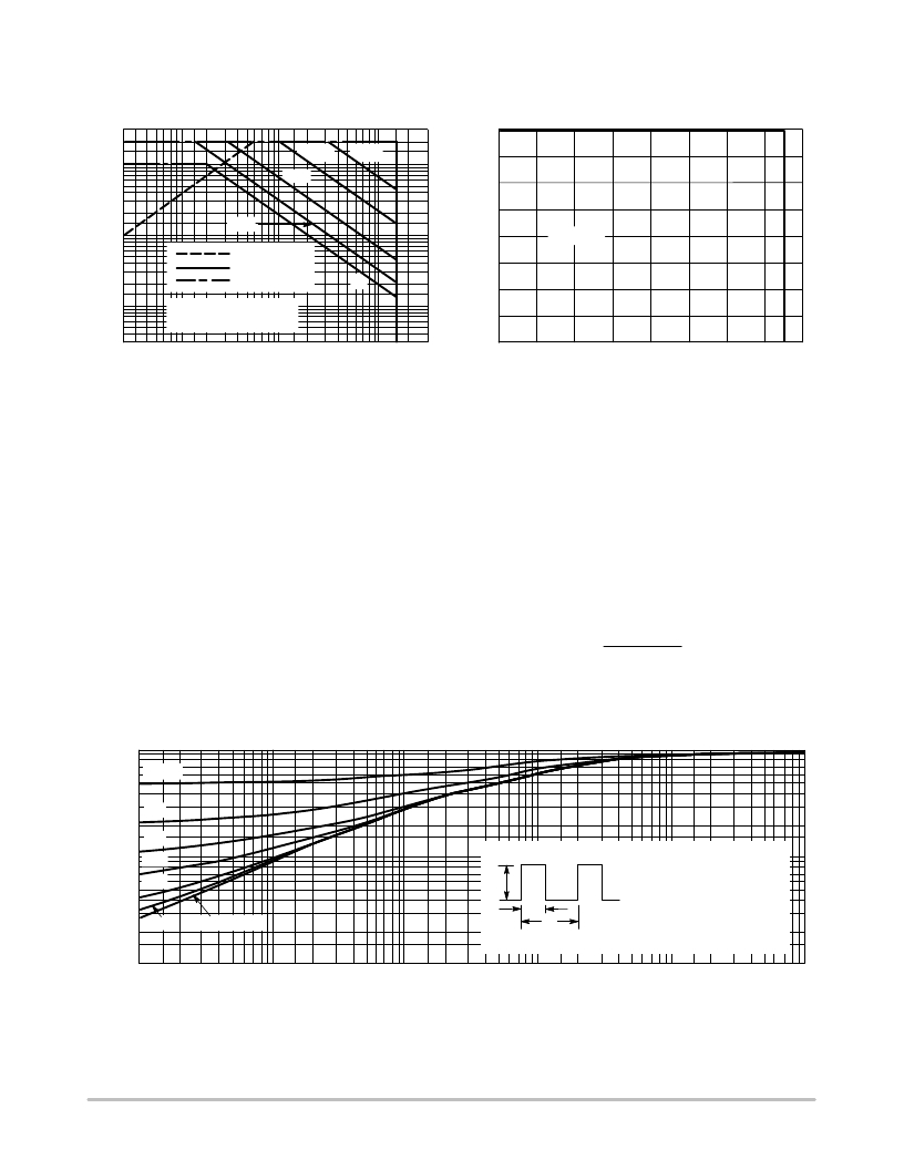
�Figure� 8.� Maximum� Rated� Forward� Biased�
�Safe� Operating� Area�
�FORWARD� BIASED� SAFE� OPERATING� AREA�
�The� FBSOA� curves� define� the� maximum� drain� ?� to� ?� source�
�voltage� and� drain� current� that� a� device� can� safely� handle�
�when� it� is� forward� biased,� or� when� it� is� on,� or� being� turned�
�on.� Because� these� curves� include� the� limitations� of�
�simultaneous� high� voltage� and� high� current,� up� to� the� rating�
�of� the� device,� they� are� especially� useful� to� designers� of� linear�
�systems.� The� curves� are� based� on� a� case� temperature� of� 25� °� C�
�and� a� maximum� junction� temperature� of� 150� °� C.� Limitations�
�for� repetitive� pulses� at� various� case� temperatures� can� be�
�determined� by� using� the� thermal� response� curves.� Motorola�
�Application� Note,� AN569,� “Transient� Thermal�
�Resistance� ?� General� Data� and� Its� Use”� provides� detailed�
�instructions.�
�V� DS� ,� DRAIN-TO-SOURCE� VOLTAGE� (VOLTS)�
�Figure� 9.� Maximum� Rated� Switching�
�Safe� Operating� Area�
�SWITCHING� SAFE� OPERATING� AREA�
�The� switching� safe� operating� area� (SOA)� of� Figure� 9� is� the�
�boundary� that� the� load� line� may� traverse� without� incurring�
�damage� to� the� MOSFET.� The� fundamental� limits� are� the�
�peak� current,� I� DM� and� the� breakdown� voltage,� V� (BR)DSS� .�
�The� switching� SOA� shown� in� Figure� 8� is� applicable� for� both�
�turn� ?� on� and� turn� ?� off� of� the� devices� for� switching� times� less�
�than� one� microsecond.�
�The� power� averaged� over� a� complete� switching� cycle�
�must� be� less� than:�
�T� J(max)� ?� T� C�
�R� q� JC�
�0.7�
�0.5�
�0.3�
�D� =� 0.5�
�0.2�
�0.2�
�0.1�
�0.1� 0.05�
�0.07�
�0.02�
�0.05�
�P� (pk)�
�R� q� JC� (t)� =� r(t)� R� q� JC�
�R� q� JC� (t)� =� 6.25� °� C/W� MAX�
�D� CURVES� APPLY� FOR� POWER�
�0.03�
�0.02�
�0.01�
�SINGLE� PULSE�
�t� 1�
�t� 2�
�DUTY� CYCLE,� D� =� t� 1� /t� 2�
�PULSE� TRAIN� SHOWN�
�READ� TIME� AT� t� 1�
�T� J(pk)� -� T� C� =� P� (pk)� R� q� JC� (t)�
�0.01�
�0.01�
�0.02� 0.03�
�0.05�
�0.1�
�0.2� 0.3�
�0.5�
�1� 2� 3� 5� 10�
�20�
�50�
�100�
�200�
�500�
�1000�
�t,� TIME� OR� PULSE� WIDTH� (ms)�
�Figure� 10.� Thermal� Response�
�http://onsemi.com�
�4�
�相关PDF资料 |
PDF描述 |
|---|---|
| MTD6N20ET4 | MOSFET N-CH 200V 6A DPAK |
| MTD6P10E | MOSFET P-CH 100V 6A DPAK |
| MTD8000N4-T | PHOTOTRANS 880NM DOME CLR TO-18 |
| MTD8600N-T | PHOTOTRANS 880NM DOME CLR TO-18 |
| MTD8600N4-T | PHOTOTRANS 880NM DOME CLR TO-18 |
相关代理商/技术参数 |
参数描述 |
|---|---|
| MTD6N15T4G | 功能描述:MOSFET NFET DPAK 150V 6A 300mOhm RoHS:否 制造商:STMicroelectronics 晶体管极性:N-Channel 汲极/源极击穿电压:650 V 闸/源击穿电压:25 V 漏极连续电流:130 A 电阻汲极/源极 RDS(导通):0.014 Ohms 配置:Single 最大工作温度: 安装风格:Through Hole 封装 / 箱体:Max247 封装:Tube |
| MTD6N15T4GV | 功能描述:MOSFET Single N-Ch 150V 6A RoHS:否 制造商:STMicroelectronics 晶体管极性:N-Channel 汲极/源极击穿电压:650 V 闸/源击穿电压:25 V 漏极连续电流:130 A 电阻汲极/源极 RDS(导通):0.014 Ohms 配置:Single 最大工作温度: 安装风格:Through Hole 封装 / 箱体:Max247 封装:Tube |
| MTD6N20 | 制造商:ON Semiconductor 功能描述:MOSFET N D-PAK |
| MTD6N20E | 制造商:Rochester Electronics LLC 功能描述:- Bulk 制造商:ON Semiconductor 功能描述: |
| MTD6N20E1 | 制造商:Rochester Electronics LLC 功能描述:- Bulk 制造商:ON Semiconductor 功能描述: |
发布紧急采购,3分钟左右您将得到回复。