- 您现在的位置:买卖IC网 > PDF目录97629 > MTV10N100E (ON SEMICONDUCTOR) 10 A, 1000 V, 1.3 ohm, N-CHANNEL, Si, POWER, MOSFET PDF资料下载
参数资料
| 型号: | MTV10N100E |
| 厂商: | ON SEMICONDUCTOR |
| 元件分类: | JFETs |
| 英文描述: | 10 A, 1000 V, 1.3 ohm, N-CHANNEL, Si, POWER, MOSFET |
| 封装: | D3PAK-3 |
| 文件页数: | 1/10页 |
| 文件大小: | 269K |
| 代理商: | MTV10N100E |
1
Motorola TMOS Power MOSFET Transistor Device Data
Designer's Data Sheet
TMOS E-FET.
Power Field Effect Transistor
D3PAK for Surface Mount
N–Channel Enhancement–Mode Silicon Gate
The D3PAK package has the capability of housing the largest chip
size of any standard, plastic, surface mount power semiconductor.
This allows it to be used in applications that require surface mount
components with higher power and lower RDS(on) capabilities. This
high voltage MOSFET uses an advanced termination scheme to
provide enhanced voltage–blocking capability without degrading
performance over time. In addition, this advanced TMOS E–FET is
designed to withstand high energy in the avalanche and commuta-
tion modes. The new energy efficient design also offers a drain–to–
source diode with a fast recovery time. Designed for high voltage,
high speed switching applications in surface mount PWM motor
controls and both ac–dc and dc–dc power supplies. These devices
are particularly well suited for bridge circuits where diode speed and
commutating safe operating areas are critical and offer additional
safety margin against unexpected voltage transients.
Robust High Voltage Termination
Avalanche Energy Specified
Source–to–Drain Diode Recovery Time Comparable to a Discrete
Fast Recovery Diode
Diode is Characterized for Use in Bridge Circuits
IDSS and VDS(on) Specified at Elevated Temperature
Short Heatsink Tab Manufactured – Not Sheared
Specifically Designed Leadframe for Maximum Power Dissipation
Available in 24 mm, 13–inch/500 Unit Tape & Reel, Add –RL Suffix to Part Number
MAXIMUM RATINGS (TC = 25°C unless otherwise noted)
Rating
Symbol
Value
Unit
Drain–to–Source Voltage
VDSS
1000
Vdc
Drain–to–Gate Voltage (RGS = 1.0 M)
VDGR
1000
Vdc
Gate–to–Source Voltage — Continuous
VGS
±20
Vdc
Drain Current — Continuous
Drain Current — Continuous @ 100
°C
Drain Current — Single Pulse (tp ≤ 10 s)
ID
IDM
10
6.2
30
Adc
Apk
Total Power Dissipation
Derate above 25
°C
Total Power Dissipation @ TC = 25°C (1)
PD
250
2.0
3.57
Watts
W/
°C
Watts
Operating and Storage Temperature Range
TJ, Tstg
– 55 to 150
°C
Single Pulse Drain–to–Source Avalanche Energy — Starting TJ = 25°C
(VDD = 100 Vdc, VGS = 10 Vdc, Peak IL = 10 Apk, L = 10 mH, RG = 25 )
EAS
500
mJ
Thermal Resistance — Junction to Case
Thermal Resistance — Junction to Ambient
Thermal Resistance — Junction to Ambient (1)
R
θJC
R
θJA
R
θJA
0.5
62.5
35
°C/W
Maximum Lead Temperature for Soldering Purposes, 1/8
″ from case for 10 seconds
TL
260
°C
(1) When surface mounted to an FR4 board using the minimum recommended pad size.
Designer’s Data for “Worst Case” Conditions — The Designer’s Data Sheet permits the design of most circuits entirely from the information presented. SOA Limit
curves — representing boundaries on device characteristics — are given to facilitate “worst case” design.
E–FET and Designer’s are trademarks of Motorola, Inc. TMOS is a registered trademark of Motorola, Inc.
Thermal Clad is a trademark of the Bergquist Company.
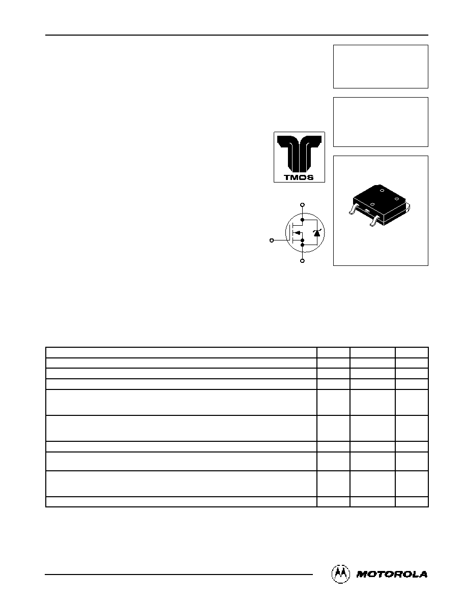
Order this document
by MTV10N100E/D
MOTOROLA
SEMICONDUCTOR TECHNICAL DATA
CASE 433–01, Style 2
D3PAK Surface Mount
MTV10N100E
TMOS POWER FET
10 AMPERES
1000 VOLTS
RDS(on) = 1.3 OHM
D
S
G
N–Channel
Motorola, Inc. 1996
相关PDF资料 |
PDF描述 |
|---|---|
| MTV10N100E-RL | 10 A, 1000 V, 1.3 ohm, N-CHANNEL, Si, POWER, MOSFET |
| MTW6N100EG | 6 A, 1000 V, 1.5 ohm, N-CHANNEL, Si, POWER, MOSFET, TO-247AE |
| MUN2112 | 100 mA, 50 V, PNP, Si, SMALL SIGNAL TRANSISTOR |
| MUN2214 | 100 mA, 50 V, NPN, Si, SMALL SIGNAL TRANSISTOR |
| MUN2212 | 100 mA, 50 V, NPN, Si, SMALL SIGNAL TRANSISTOR |
相关代理商/技术参数 |
参数描述 |
|---|---|
| MTV1-100SL1 | 制造商:ITT Interconnect Solutions 功能描述:MTV1-100SL1 - Bulk |
| MTV1-102SL1 | 制造商:ITT Interconnect Solutions 功能描述:MTV1-102SL1 - Bulk |
| MTV1-102SS | 制造商:ITT Interconnect Solutions 功能描述:MTV1-102SS - Bulk |
| MTV1-104PL1 | 制造商:ITT Interconnect Solutions 功能描述:MTV1-104PL1 - Bulk |
| MTV1-104SL1 | 制造商:ITT Interconnect Solutions 功能描述:MTV1-104SL1 - Bulk |
发布紧急采购,3分钟左右您将得到回复。