- 您现在的位置:买卖IC网 > PDF目录96108 > MTW45N10E (ON SEMICONDUCTOR) 45 A, 100 V, 0.035 ohm, N-CHANNEL, Si, POWER, MOSFET, TO-247AE PDF资料下载
参数资料
| 型号: | MTW45N10E |
| 厂商: | ON SEMICONDUCTOR |
| 元件分类: | JFETs |
| 英文描述: | 45 A, 100 V, 0.035 ohm, N-CHANNEL, Si, POWER, MOSFET, TO-247AE |
| 封装: | CASE 340K-01, 3 PIN |
| 文件页数: | 5/8页 |
| 文件大小: | 62K |
| 代理商: | MTW45N10E |
MTW45N10E
http://onsemi.com
5
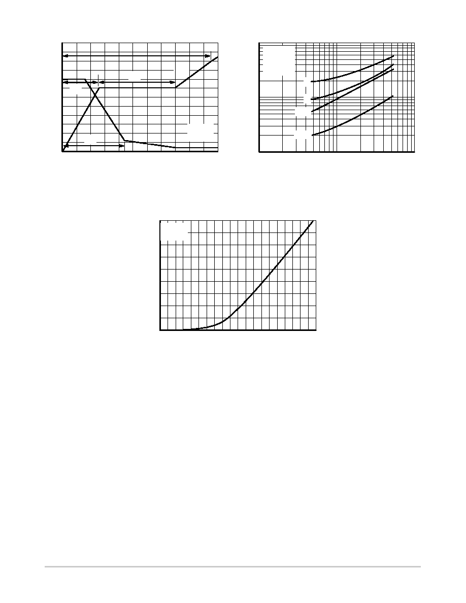
DRAIN–TO–SOURCE DIODE CHARACTERISTICS
0.5
0.62
0.74
0.86
0.98
1.1
0
15
25
35
45
VSD, SOURCE-TO-DRAIN VOLTAGE (VOLTS)
Figure 8. Gate–To–Source and Drain–To–Source
Voltage versus Total Charge
I S
,SOURCE
CURRENT
(AMPS)
Figure 9. Resistive Switching Time
Variation versus Gate Resistance
RG, GATE RESISTANCE (OHMS)
1
10
100
1000
100
10
t,TIME
(ns)
VDD = 50 V
ID = 45 A
VGS = 10 V
TJ = 25°C
tr
tf
td(off)
td(on)
VGS = 0 V
TJ = 25°C
Figure 10. Diode Forward Voltage versus Current
120
V GS
,GA
TE-T
O-SOURCE
VOL
TAGE
(VOL
TS)
100
80
60
40
20
0
10
6
2
0
QT, TOTAL CHARGE (nC)
VDS
,DRAIN-T
O-SOURCE
VOL
TAGE
(VOL
TS)
12
8
4
20
40
60
80
110
VDS
VGS
Q1
Q2
10
30
50
70
90
0.56
0.68
0.80
0.92
1.04
100
10
20
30
40
5
QT
Q3
ID = 45 A
TJ = 25°C
SAFE OPERATING AREA
The Forward Biased Safe Operating Area curves define
the maximum simultaneous drain–to–source voltage and
drain current that a transistor can handle safely when it is
forward biased. Curves are based upon maximum peak
junction temperature and a case temperature (TC) of 25°C.
Peak repetitive pulsed power limits are determined by using
the thermal response data in conjunction with the procedures
discussed
in
AN569,
“Transient
Thermal
Resistance–General Data and Its Use.”
Switching between the off–state and the on–state may
traverse any load line provided neither rated peak current
(IDM) nor rated voltage (VDSS) is exceeded and the
transition time (tr,tf) do not exceed 10 s. In addition the total
power averaged over a complete switching cycle must not
exceed (TJ(MAX) – TC)/(R
θJC).
A Power MOSFET designated E–FET can be safely used
in switching circuits with unclamped inductive loads. For
reliable operation, the stored energy from circuit inductance
dissipated in the transistor while in avalanche must be less
than the rated limit and adjusted for operating conditions
differing from those specified. Although industry practice is
to rate in terms of energy, avalanche energy capability is not
a constant. The energy rating decreases non–linearly with an
increase of peak current in avalanche and peak junction
temperature.
Although many E–FETs can withstand the stress of
drain–to–source avalanche at currents up to rated pulsed
current (IDM), the energy rating is specified at rated
continuous current (ID), in accordance with industry
custom. The energy rating must be derated for temperature
as shown in the accompanying graph (Figure 12). Maximum
energy at currents below rated continuous ID can safely be
assumed to equal the values indicated.
相关PDF资料 |
PDF描述 |
|---|---|
| MTW7N80E | 7 A, 800 V, 1 ohm, N-CHANNEL, Si, POWER, MOSFET, TO-247AE |
| MTY100N10E | 100 A, 100 V, 0.011 ohm, N-CHANNEL, Si, POWER, MOSFET, TO-264AA |
| MTZJ33B | 33 V, 0.5 W, SILICON, UNIDIRECTIONAL VOLTAGE REGULATOR DIODE, DO-34 |
| MTZJ36B | 36 V, 0.5 W, SILICON, UNIDIRECTIONAL VOLTAGE REGULATOR DIODE, DO-34 |
| MTZJ4.7B | 4.7 V, 0.5 W, SILICON, UNIDIRECTIONAL VOLTAGE REGULATOR DIODE, DO-34 |
相关代理商/技术参数 |
参数描述 |
|---|---|
| MTW4N80 | 制造商:MOTOROLA 制造商全称:Motorola, Inc 功能描述:TMOS E-FET POWER FIELD EFFECT TRANSISITOR N-CHANNEL ENHANCEMENT-MODE SILICON GATE |
| MTW4N80E | 制造商:MOTOROLA 制造商全称:Motorola, Inc 功能描述:TMOS E-FET POWER FIELD EFFECT TRANSISITOR N-CHANNEL ENHANCEMENT-MODE SILICON GATE |
| MTW54N05E | 制造商:MOTOROLA 制造商全称:Motorola, Inc 功能描述:High Energy in the Avalanche and Commutation modes |
| MTW6051212 | 制造商:TDK-Lambda Corporation 功能描述:AC/DC PS TRIPLE-OUT 5V/12V/-12V 5A/2.5A/0.5A 60W - Bulk 制造商:TDK 功能描述:AC/DC CONVERT 5V +/-12V 60W |
| MTW60-51212 | 功能描述:线性和开关式电源 60W 5V 12V RoHS:否 制造商:TDK-Lambda 产品:Switching Supplies 开放式框架/封闭式:Enclosed 输出功率额定值:800 W 输入电压:85 VAC to 265 VAC 输出端数量:1 输出电压(通道 1):20 V 输出电流(通道 1):40 A 商用/医用: 输出电压(通道 2): 输出电流(通道 2): 安装风格:Rack 长度: 宽度: 高度: |
发布紧急采购,3分钟左右您将得到回复。