- 您现在的位置:买卖IC网 > PDF目录98049 > MUN5233T3 (ON SEMICONDUCTOR) 100 mA, 50 V, NPN, Si, SMALL SIGNAL TRANSISTOR PDF资料下载
参数资料
| 型号: | MUN5233T3 |
| 厂商: | ON SEMICONDUCTOR |
| 元件分类: | 小信号晶体管 |
| 英文描述: | 100 mA, 50 V, NPN, Si, SMALL SIGNAL TRANSISTOR |
| 封装: | SC-70, 3 PIN |
| 文件页数: | 1/39页 |
| 文件大小: | 377K |
| 代理商: | MUN5233T3 |
当前第1页第2页第3页第4页第5页第6页第7页第8页第9页第10页第11页第12页第13页第14页第15页第16页第17页第18页第19页第20页第21页第22页第23页第24页第25页第26页第27页第28页第29页第30页第31页第32页第33页第34页第35页第36页第37页第38页第39页
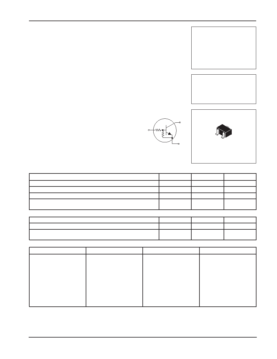
PIN3
COLLECTOR
(OUTPUT)
PIN2
EMITTER
(GROUND)
PIN1
BASE
(INPUT)
R1
R2
2–769
Motorola Small–Signal Transistors, FETs and Diodes Device Data
Bias Resistor Transistor
NPN Silicon Surface Mount Transistor with
Monolithic Bias Resistor Network
This new series of digital transistors is designed to replace a single device
and its external resistor bias network. The BRT (Bias Resistor Transistor)
contains a single transistor with a monolithic bias network consisting of two
resistors; a series base resistor and a base-emitter resistor. The BRT eliminates
these individual components by integrating them into a single device. The use
of a BRT can reduce both system cost and board space. The device is housed
in the SC-70/SOT-323 package which is designed for low power surface mount
applications.
Simplifies Circuit Design
Reduces Board Space
Reduces Component Count
The SC-70/SOT-323 package can be soldered using
wave or reflow. The modified gull-winged leads absorb
thermal stress during soldering eliminating the possibility
of damage to the die.
Available in 8 mm embossed tape and reel
Use the Device Number to order the 7 inch/3000 unit reel.
Replace “T1” with “T3” in the Device Number to order the
13 inch/10,000 unit reel.
MAXIMUM RATINGS (TA = 25°C unless otherwise noted)
Rating
Symbol
Value
Unit
Collector-Base Voltage
VCBO
50
Vdc
Collector-Emitter Voltage
VCEO
50
Vdc
Collector Current
IC
100
mAdc
Total Power Dissipation @ TA = 25°C(1)
Derate above 25
°C
PD
*150
1.2
mW
mW/
°C
THERMAL CHARACTERISTICS
Thermal Resistance — Junction-to-Ambient (surface mounted)
R
θJA
833
°C/W
Operating and Storage Temperature Range
TJ, Tstg
– 65 to +150
°C
Maximum Temperature for Soldering Purposes,
Time in Solder Bath
TL
260
10
°C
Sec
DEVICE MARKING AND RESISTOR VALUES
Device
Marking
R1 (K)
R2 (K)
MUN5211T1
MUN5212T1
MUN5213T1
MUN5214T1
MUN5215T1(2)
8A
8B
8C
8D
8E
10
22
47
10
22
47
∞
MUN5216T1(2)
MUN5230T1(2)
MUN5231T1(2)
MUN5232T1(2)
MUN5233T1(2)
MUN5234T1(2)
8F
8G
8H
8J
8K
8L
4.7
1.0
2.2
4.7
22
∞
1.0
2.2
4.7
47
1. Device mounted on a FR-4 glass epoxy printed circuit board using the minimum recommended footprint.
2. New devices. Updated curves to follow in subsequent data sheets.
Preferred devices are Motorola recommended choices for future use and best overall value.
MOTOROLA
SEMICONDUCTOR TECHNICAL DATA
NPN SILICON
BIAS RESISTOR
TRANSISTORS
Motorola Preferred Devices
CASE 419-02, STYLE 3
SC-70/SOT-323
MUN5211T1
SERIES
1
2
3
REV 2
相关PDF资料 |
PDF描述 |
|---|---|
| MUN5231T3 | 100 mA, 50 V, NPN, Si, SMALL SIGNAL TRANSISTOR |
| MUN5214T3 | 100 mA, 50 V, NPN, Si, SMALL SIGNAL TRANSISTOR |
| MUN5216T3 | 100 mA, 50 V, NPN, Si, SMALL SIGNAL TRANSISTOR |
| MUN5311DW1T2 | 100 mA, 50 V, 2 CHANNEL, NPN AND PNP, Si, SMALL SIGNAL TRANSISTOR |
| MUN5313DW1T2 | 100 mA, 50 V, 2 CHANNEL, NPN AND PNP, Si, SMALL SIGNAL TRANSISTOR |
相关代理商/技术参数 |
参数描述 |
|---|---|
| MUN5234 | 制造商:ONSEMI 制造商全称:ON Semiconductor 功能描述:Dual Bias Resistor Transistors |
| MUN5234DW | 制造商:WEITRON 制造商全称:Weitron Technology 功能描述:Surface Mount Dual Bias Resistor Transistor |
| MUN5234DW1T1 | 功能描述:开关晶体管 - 偏压电阻器 100mA 50V BRT Dual RoHS:否 制造商:ON Semiconductor 配置: 晶体管极性:NPN/PNP 典型输入电阻器: 典型电阻器比率: 安装风格:SMD/SMT 封装 / 箱体: 直流集电极/Base Gain hfe Min:200 mA 最大工作频率: 集电极—发射极最大电压 VCEO:50 V 集电极连续电流:150 mA 峰值直流集电极电流: 功率耗散:200 mW 最大工作温度: 封装:Reel |
| MUN5234DW1T1G | 功能描述:开关晶体管 - 偏压电阻器 100mA 50V BRT Dual NPN RoHS:否 制造商:ON Semiconductor 配置: 晶体管极性:NPN/PNP 典型输入电阻器: 典型电阻器比率: 安装风格:SMD/SMT 封装 / 箱体: 直流集电极/Base Gain hfe Min:200 mA 最大工作频率: 集电极—发射极最大电压 VCEO:50 V 集电极连续电流:150 mA 峰值直流集电极电流: 功率耗散:200 mW 最大工作温度: 封装:Reel |
| MUN5234T1 | 功能描述:开关晶体管 - 偏压电阻器 100mA 50V BRT NPN RoHS:否 制造商:ON Semiconductor 配置: 晶体管极性:NPN/PNP 典型输入电阻器: 典型电阻器比率: 安装风格:SMD/SMT 封装 / 箱体: 直流集电极/Base Gain hfe Min:200 mA 最大工作频率: 集电极—发射极最大电压 VCEO:50 V 集电极连续电流:150 mA 峰值直流集电极电流: 功率耗散:200 mW 最大工作温度: 封装:Reel |
发布紧急采购,3分钟左右您将得到回复。